TI사에서 제공하는 28335 예제들의 메인을 보다보면
#include "DSP28x_Project.h"     // Device Headerfile and Examples Include File

__interrupt void cpu_timer0_isr(void);
__interrupt void cpu_timer1_isr(void);
__interrupt void cpu_timer2_isr(void);

void main(void)
{

   InitSysCtrl();

   DINT;
   InitPieCtrl();

   IER = 0x0000;
   IFR = 0x0000;

   InitPieVectTable();

   EALLOW;  // This is needed to write to EALLOW protected registers
   PieVectTable.TINT0 = &cpu_timer0_isr;
   PieVectTable.XINT13 = &cpu_timer1_isr;
   PieVectTable.TINT2 = &cpu_timer2_isr;
   EDIS;    // This is needed to disable write to EALLOW protected registers

   InitCpuTimers();   // For this example, only initialize the Cpu Timers

#if (CPU_FRQ_150MHZ)
   ConfigCpuTimer(&CpuTimer0, 150, 1000000);
   ConfigCpuTimer(&CpuTimer1, 150, 1000000);
   ConfigCpuTimer(&CpuTimer2, 150, 1000000);
#endif

#if (CPU_FRQ_100MHZ)

   ConfigCpuTimer(&CpuTimer0, 100, 1000000);
   ConfigCpuTimer(&CpuTimer1, 100, 1000000);
   ConfigCpuTimer(&CpuTimer2, 100, 1000000);
#endif

   CpuTimer0Regs.TCR.all = 0x4000; // Use write-only instruction to set TSS bit = 0
   CpuTimer1Regs.TCR.all = 0x4000; // Use write-only instruction to set TSS bit = 0
   CpuTimer2Regs.TCR.all = 0x4000; // Use write-only instruction to set TSS bit = 0

   IER |= M_INT1;
   IER |= M_INT13;
   IER |= M_INT14;

   PieCtrlRegs.PIEIER1.bit.INTx7 = 1;

   EINT;   // Enable Global interrupt INTM
   ERTM;   // Enable Global realtime interrupt DBGM

   for(;;);
}

__interrupt void cpu_timer0_isr(void)
{
   CpuTimer0.InterruptCount++;
   PieCtrlRegs.PIEACK.all = PIEACK_GROUP1;
}

__interrupt void cpu_timer1_isr(void)
{
   CpuTimer1.InterruptCount++;
   EDIS;
}

__interrupt void cpu_timer2_isr(void)
{  EALLOW;
   CpuTimer2.InterruptCount++;
   EDIS;
}
위 코드 에서와 같이 InitSysCtrl()라는 함수가 항상 먼저 선언된다.
InitSysCtrl()
//
// InitSysCtrl - This function initializes the System Control registers to a
// known state.
// - Disables the watchdog
// - Set the PLLCR for proper SYSCLKOUT frequency
// - Set the pre-scaler for the high and low frequency peripheral clocks
// - Enable the clocks to the peripherals
//
void
InitSysCtrl(void)
{
    //
    // Disable the watchdog
    //
    DisableDog();

    //
    // Initialize the PLL control: PLLCR and DIVSEL
    // DSP28_PLLCR and DSP28_DIVSEL are defined in DSP2833x_Examples.h
    //
    InitPll(DSP28_PLLCR,DSP28_DIVSEL);

    //
    // Initialize the peripheral clocks
    //
    InitPeripheralClocks();
}
InitSysCtrl() 함수의 내용을 살펴보면 크게 3가지의 함수로 이루어져 있으며 주석에 대한 설명으론
STEP 1 : Watchdog OFF
STEP 2 : PLLCR 레지스터를 설정하여 SYSCLKOUT을 생성
STEP 3 : pre_scaler를 설정하여 고속 주변장치 클럭과 저속 주변장치 클럭을 조정
STEP 4 : 클럭 ON 하여 주변장치에 공급
의 순서로 작동된다.
이중 InitPll()를 살펴보고자 한다.
InitPll()
InitPll(DSP28_PLLCR,DSP28_DIVSEL);void
InitPll(Uint16 val, Uint16 divsel)
{
//
// Make sure the PLL is not running in limp mode
//
if (SysCtrlRegs.PLLSTS.bit.MCLKSTS != 0)
{
//
// Missing external clock has been detected
// Replace this line with a call to an appropriate
// SystemShutdown(); function.
//
asm(" ESTOP0");
}
//
// DIVSEL MUST be 0 before PLLCR can be changed from
// 0x0000. It is set to 0 by an external reset XRSn
// This puts us in 1/4
//
if (SysCtrlRegs.PLLSTS.bit.DIVSEL != 0)
{
EALLOW;
SysCtrlRegs.PLLSTS.bit.DIVSEL = 0;
EDIS;
}
//
// Change the PLLCR
//
if (SysCtrlRegs.PLLCR.bit.DIV != val)
{
EALLOW;
//
// Before setting PLLCR turn off missing clock detect logic
//
SysCtrlRegs.PLLSTS.bit.MCLKOFF = 1;
SysCtrlRegs.PLLCR.bit.DIV = val;
EDIS;
//
// Optional: Wait for PLL to lock.
// During this time the CPU will switch to OSCCLK/2 until
// the PLL is stable. Once the PLL is stable the CPU will
// switch to the new PLL value.
//
// This time-to-lock is monitored by a PLL lock counter.
//
// Code is not required to sit and wait for the PLL to lock.
// However, if the code does anything that is timing critical,
// and requires the correct clock be locked, then it is best to
// wait until this switching has completed.
//
//
// Wait for the PLL lock bit to be set.
//
//
// The watchdog should be disabled before this loop, or fed within
// the loop via ServiceDog().
//
//
// Uncomment to disable the watchdog
//
DisableDog();
while(SysCtrlRegs.PLLSTS.bit.PLLLOCKS != 1)
{
//
// Uncomment to service the watchdog
//
//ServiceDog();
}
EALLOW;
SysCtrlRegs.PLLSTS.bit.MCLKOFF = 0;
EDIS;
}
//
// If switching to 1/2
//
if((divsel == 1)||(divsel == 2))
{
EALLOW;
SysCtrlRegs.PLLSTS.bit.DIVSEL = divsel;
EDIS;
}
//
// NOTE: ONLY USE THIS SETTING IF PLL IS BYPASSED (I.E. PLLCR = 0) OR OFF
// If switching to 1/1
// * First go to 1/2 and let the power settle
// The time required will depend on the system, this is only an example
// * Then switch to 1/1
//
if(divsel == 3)
{
EALLOW;
SysCtrlRegs.PLLSTS.bit.DIVSEL = 2;
DELAY_US(50L);
SysCtrlRegs.PLLSTS.bit.DIVSEL = 3;
EDIS;
}
}순서대로 설명하자면
SysCtrlRegs.PLLSTS.bit.MCLKSTS : PLLSTS의 MCLKSTS가 0인지 확인 한다.
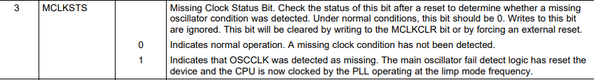
항상 0으로 읽히는 것을 가정으로 작동하며 만약 0이 아닌 다른값 (1) 이 읽힐 경우 내부적으로 실행과정에서의 이상을 감지하여 자체적으로 칩의 작동을 Reset하는 asm(" ESTOP0"); 이라는 어셈블리 명령어를 실행한다. 이를 통해 칩의 첫 실행과정에서 발생하는 오류를 대비할 수 있다.
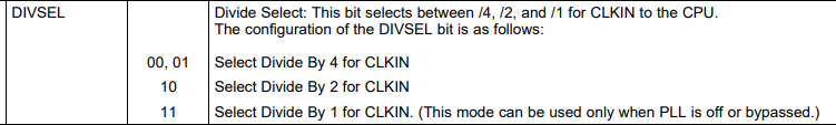
SysCtrlRegs.PLLSTS.bit.DIVSEL : PLLSTS의 DIVSEL이 0인지 확인 한다.
이는 에뮬레이터를 사용시 전원의 연결만을 통해서 이미 PLL이 작동하기 떄문에 그냥 실행히 어떤 동작을 할지 예상이 불가하다 이를 방지하기 위해 TI사에서는 0 입력을 권장하기 때문에 값이 0 이 아닌경우
EALLOW를 통해 레지스터 보호를 풀어 수정하고 다시 EDIS를 통해 레지스터를 보호하는 과정을 거친다.
EALLOW와 EDIS
28335를 구성하는 레지스터들중 일부는 함부로 수정하면 작동에 영향을 주는 레지스터들이 존재한다. 따라서 이를 보호하기 위하여 기본적으로 레지스터들은 보호되어 있는 상태이다. 만냑 수정을 원할경우 레지스터 제어전 EALLOW()를 선언하여 보호를 풀고 수정해야한다. 그리고 레지스터 수정완료 후에는 EDIS를 통해 레시스터들을 다시 보호하게끔 해두어야 한다.- 보호되는 레지스터들
• Device Emulation Registers
• Flash Registers
• CSM Registers
• PIE Vector Table
• System Control Registers
• GPIO MUX Registers
• Certain eCAN Registers
• XINTF Registers
if (SysCtrlRegs.PLLCR.bit.DIV != val) 부분
 if (SysCtrlRegs.PLLCR.bit.DIV != val)
    {
        EALLOW;

        SysCtrlRegs.PLLSTS.bit.MCLKOFF = 1;
        SysCtrlRegs.PLLCR.bit.DIV = val;
        EDIS;

        DisableDog();

        while(SysCtrlRegs.PLLSTS.bit.PLLLOCKS != 1)
        {
            // Uncomment to service the watchdog
            //ServiceDog();
        }

        EALLOW;
        SysCtrlRegs.PLLSTS.bit.MCLKOFF = 0;
        EDIS;
    }
    ...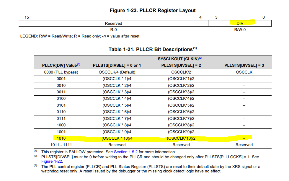
조건식을 보면 SysCtrlRegs.PLLCR.bit.DIV != val
이떄의 val값은 맨위의 매개변수로 DSP28_PLLCR,DSP28_DIVSEL 값은 다음과 같이 define 되어있다.
#define DSP28_DIVSEL     2 // Enable /2 for SYSCLKOUT

#define DSP28_PLLCR   10
따라서 DIV의 값이 10이냐 (1010)를 판단 후 비교하여 맞치 않을 경우 MCLKOFF(마스터 클럭)을 한다.
그후 DIV의 값을 내가 원하는 클럭의 조건으로 변경 후 PLL 작동이 시작된다. (다음 조건식 만족시까지)
    while(SysCtrlRegs.PLLSTS.bit.PLLLOCKS != 1)
    {
        // Uncomment to service the watchdog
        //ServiceDog();
    }

    EALLOW;
    SysCtrlRegs.PLLSTS.bit.MCLKOFF = 0;
    EDIS;
PLLSTS의 PLLLOCKS의 값이 1이 될때까지 무한 루프가 된다
PLLLOCKS : PLL이 동작시(진행중)에는 0, 완료시 값이 1이 될떄까지 대기

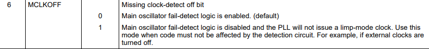
MCLKOFF : PLL 동작이 완료 되어 PLL출력 클러 오류 감지를 다시 시작
    if((divsel == 1)||(divsel == 2))
    {
        EALLOW;
        SysCtrlRegs.PLLSTS.bit.DIVSEL = divsel;
        EDIS;
    }

    //
    // NOTE: ONLY USE THIS SETTING IF PLL IS BYPASSED (I.E. PLLCR = 0) OR OFF
    // If switching to 1/1
    // * First go to 1/2 and let the power settle
    //   The time required will depend on the system, this is only an example
    // * Then switch to 1/1
    //
    if(divsel == 3)
    {
        EALLOW;
        SysCtrlRegs.PLLSTS.bit.DIVSEL = 2;
        DELAY_US(50L);
        SysCtrlRegs.PLLSTS.bit.DIVSEL = 3;
        EDIS;
    }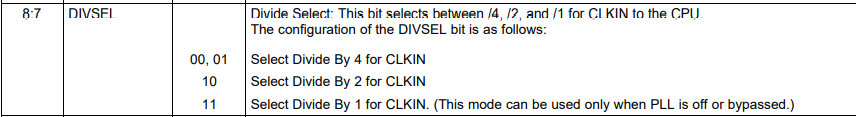
PLL 출력의 분주비를 설정
이때 조건 3일때 2번 거치는 이유는 3일떄의 DIVSEL은 PLL 클럭이 한번에 들어가므로 순간적으로 입력을 받아 오류 발생 방지를 위해 나눠서 입력을 해준다.
(PLL 은 300MHz가 가능한데 반해 28335는 150MHz까지 가능)
해당 코드에서는 /2 를 사용하였다.
InitPLL()이 실행되지 않을 경우
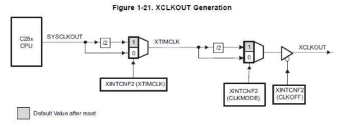
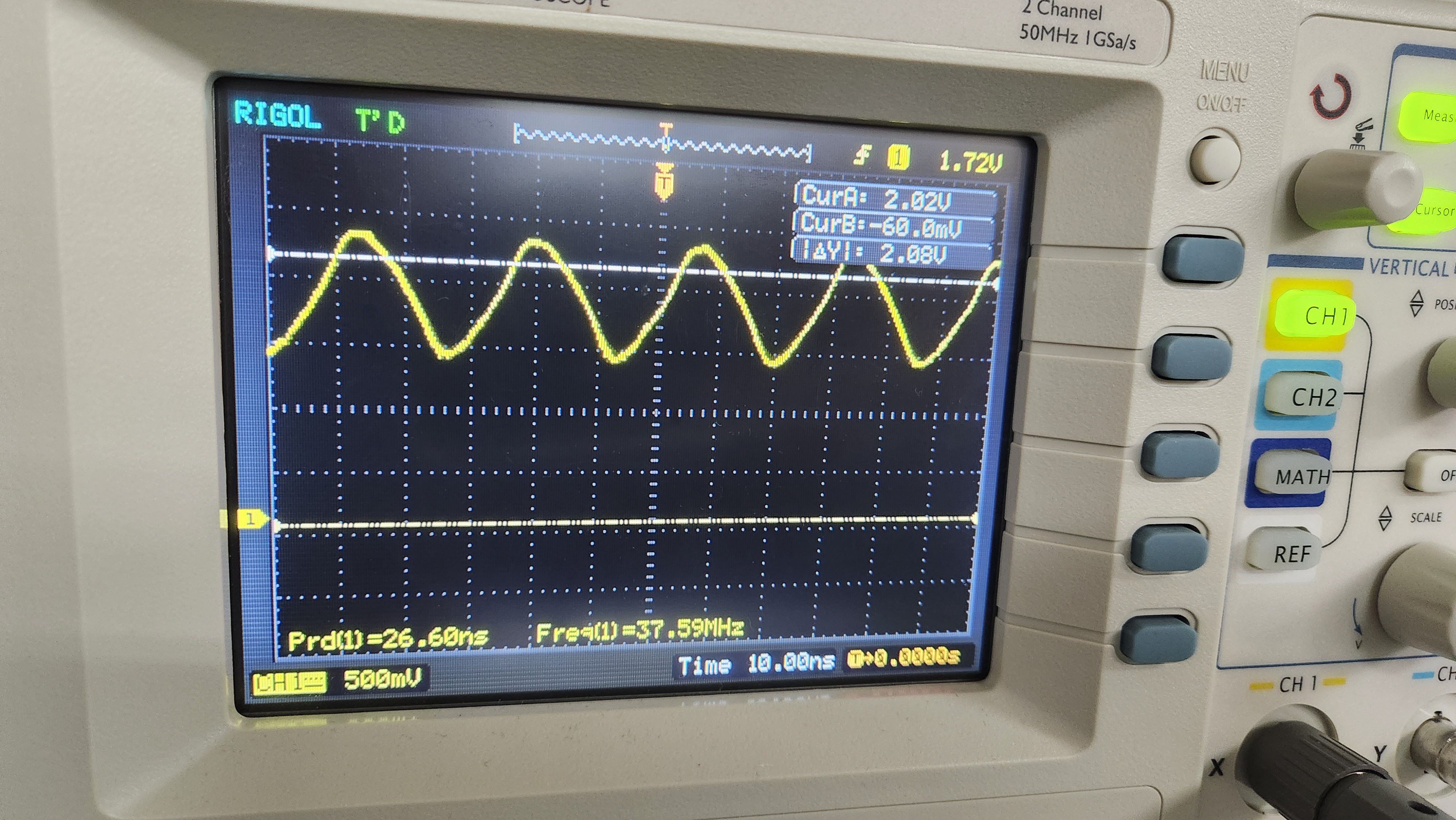
XCLKOUT은 외부 핀이고 그에 해당되는 XINTCNF2 레지스터값을 변경해주지 않는다면
(7.5MHz/2)/2=7.5MHz /4 가 외부로 출력
정상일 경우 =150MHz/4=37.5MHz
만약 코드 DisableDog();가 없을시 자체 내부적으로 Reset일 걸리게된다.
끝으로 SysCtrlRegs에 대한 내용
volatile struct SYS_CTRL_REGS SysCtrlRegs;struct SYS_CTRL_REGS {
Uint16 rsvd1; // 0
union PLLSTS_REG PLLSTS; // 1
Uint16 rsvd2[8]; // 2-9
//
// 10: High-speed peripheral clock pre-scaler
//
union HISPCP_REG HISPCP;
union LOSPCP_REG LOSPCP; // 11: Low-speed peripheral clock pre-scaler
union PCLKCR0_REG PCLKCR0; // 12: Peripheral clock control register
union PCLKCR1_REG PCLKCR1; // 13: Peripheral clock control register
union LPMCR0_REG LPMCR0; // 14: Low-power mode control register 0
Uint16 rsvd3; // 15: reserved
union PCLKCR3_REG PCLKCR3; // 16: Peripheral clock control register
union PLLCR_REG PLLCR; // 17: PLL control register
//
// No bit definitions are defined for SCSR because
// a read-modify-write instruction can clear the WDOVERRIDE bit
//
Uint16 SCSR; // 18: System control and status register
Uint16 WDCNTR; // 19: WD counter register
Uint16 rsvd4; // 20
Uint16 WDKEY; // 21: WD reset key register
Uint16 rsvd5[3]; // 22-24
//
// No bit definitions are defined for WDCR because
// the proper value must be written to the WDCHK field
// whenever writing to this register.
//
Uint16 WDCR; // 25: WD timer control register
Uint16 rsvd6[4]; // 26-29
union MAPCNF_REG MAPCNF; // 30: Dual-mapping configuration register
Uint16 rsvd7[1]; // 31
};union PLLSTS_REG {
Uint16 all;
struct PLLSTS_BITS bit;
};struct PLLSTS_BITS { // bits description
Uint16 PLLLOCKS:1; // 0 PLL lock status
Uint16 rsvd1:1; // 1 reserved
Uint16 PLLOFF:1; // 2 PLL off bit
Uint16 MCLKSTS:1; // 3 Missing clock status bit
Uint16 MCLKCLR:1; // 4 Missing clock clear bit
Uint16 OSCOFF:1; // 5 Oscillator clock off
Uint16 MCLKOFF:1; // 6 Missing clock detect
Uint16 DIVSEL:2; // 7 Divide Select
Uint16 rsvd2:7; // 15:7 reserved
};
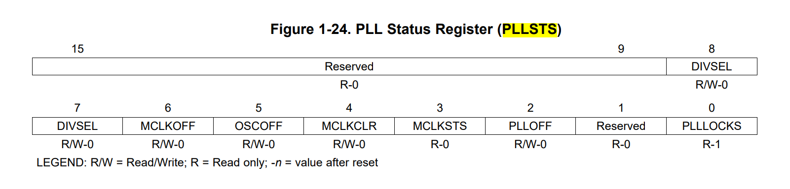
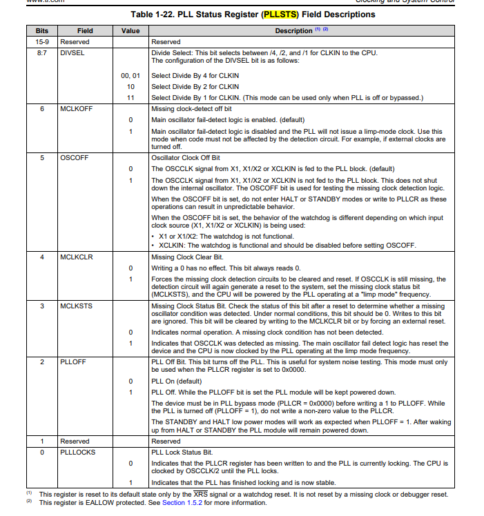
제공되는 유저 메뉴얼과 정의된 명령어들의 비트 구성이 완벽하게 일치한다.
