안녕하세요 오늘은 드디어 Circuits편에 들어왔습니다...!
길고 긴 Verilog Language편이 끝나고 Circuit편의 combinational logic을 다루어볼까합니다.
순서가 Circuit편이 먼저인듯 하나...HDLBits의 순서대로 진행하다 보니..
네 그렇게 되었습니다
사실 Verilog Language편에서 다룬 내용들도 있기 때문에 쉬운 내용들은 간단하게 언급만하고 넘어가도록 하겠습니다.
(혹시나 무슨 말인지 모르겠다 하신다면 댓글을 남겨주시면 답변드리겠습니다!!)
Wire
 그림1 : wire
이번 문제는 wire로 in out을 연결해봐라는 내용입니다.
너무 easy합니다.
module top_module (
    input in,
    output out);

    assign out = in;

endmodule
GND
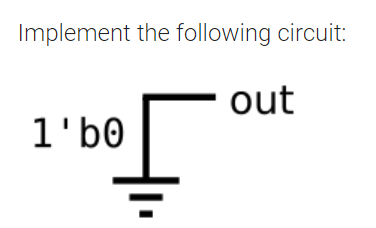 그림2 : GND
이 문제에서는 output에 ground를 연결한 것을 작성하라고 합니다.
ground는 기준 전위로 0V입니다.
logic으로 나타내면 low이며 1'b0으로 작성하면 간단하게 표현가능하답니다.
module top_module (
    output out);

    assign out = 1'b0;

endmodule
어떤가요 간단하기 않은가요?
사실 이런 회로를 작성하지는 않고 mux의 제어에 따라 GND를 출력으로 보내거나 다른 출력을 보내는 것으로 작성합니다만, 여기서는 일단해보라는 의미인 듯합니다.
NOR
이번은 NOR gate입니다.
여러분 OR gate에 대해 아시죠?
OR gate의 출력에 NOT gate를 연결해준 것이 NOR gate입니다.
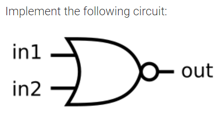 그림3 : NOR gate
자 NOR gate에 대해서만 언급하고 가면 아쉽겠지요?
그건 다음문제에서 다루겠습니다!
module top_module (
    input in1,
    input in2,
    output out);

    assign out = ~(in1|in2);

endmodule
Anoter gate
이번에는 이거 무슨 gate인지 모르겠지요..?
그냥 AND gate에서 한쪽 입력에 NOT gate를 연결해준 모습입니다.
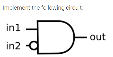 그림4 : Another gate
이 회로를 verilog로 작성하면 아래와 같습니다
module top_module (
    input in1,
    input in2,
	output out);

    assign out = in1&~in2;

endmodule
그냥 이렇게만 하고 넘어가면 조금 아쉽겠지요?
그래서 코너 속 코너를 진행하려고 합니다.
그것은 바로....and,or,not..등 gate들에 대한 연산자에 대해 조금 더 소개해보겠습니다.
operator
제가 간단하게 Vivado tool을 사용해서 아래에 있는 코드를 작성하고 합성을 한 후 나온 것을 RTL viewer로 본 것입니다
module Basic_operators(
input in1,
input in2,
output And,
output Or,
output Not,
output Xor,
output Nand,
output Nor
);
assign And = in1&in2;
assign Or = in1|in2;
assign Not = ~in1;
assign Xor = in1^in2;
assign Nand = ~(in1&in2);
assign Nor = ~(in1|in2);
endmodule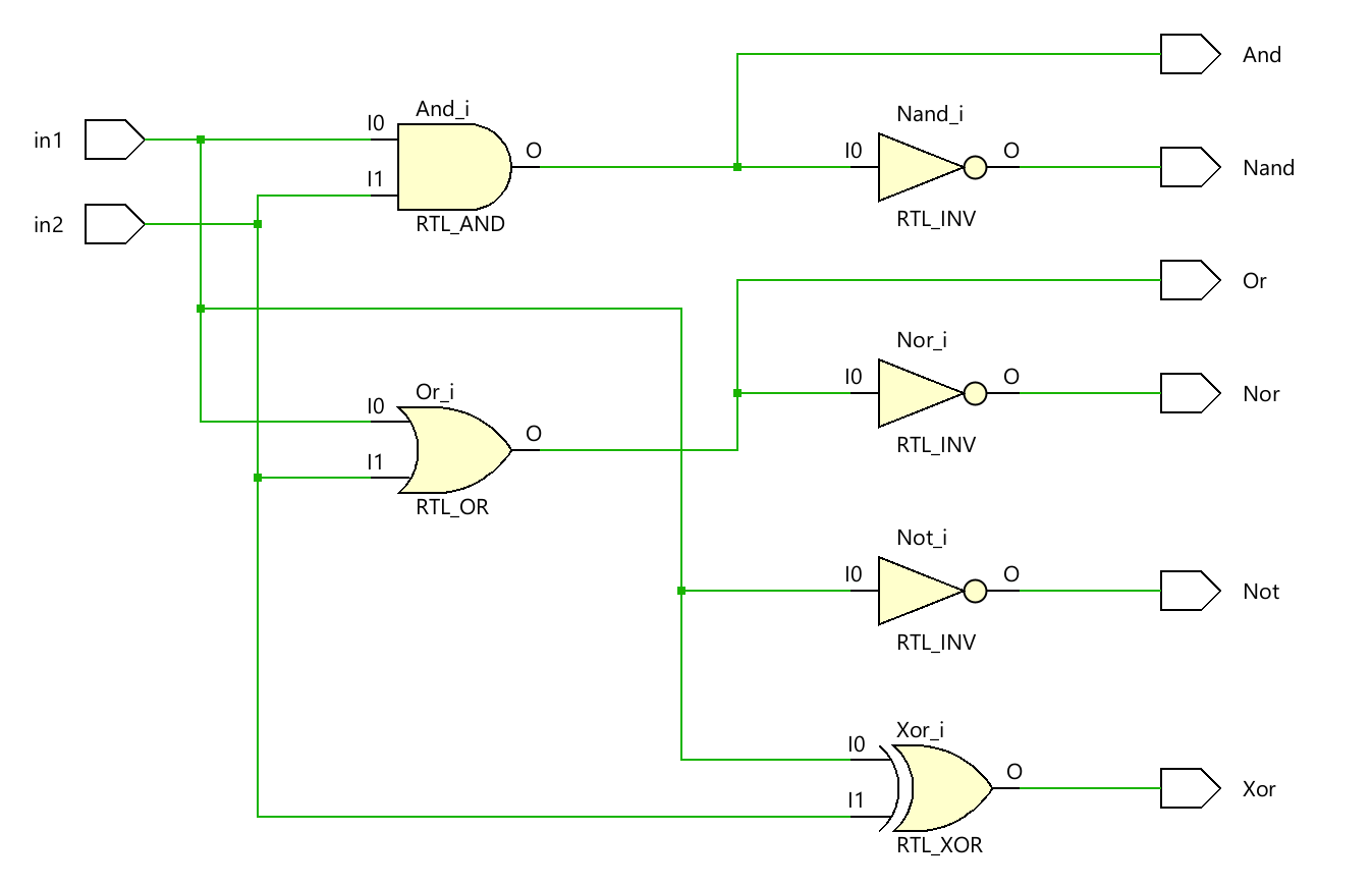 그림5 : 1bit RTL view 결과
제가 이렇게 보여드린 이유는 연산자가 gate로 합성되는 것을 보여드리면 이해를 좀 더 도와드릴 수 있을 거 같아서 이렇게 작성하였습니다.
그림과 코드상 연산자의 대조를 위해 output port의 출력이름을 해당 gate이름으로 했으니, 한번 보도록 합시다.
이건 지금 1bit 신호이기 때문에 logical operator, bitwise operator를 사용해도 결과는 동일합니다.
이게 bit가 1개가 아닌 경우 어떻게 되는지 한번 보도록 합시다.
multi bit operator
module multi_bit_operators(
input [31:0] in1,
input [31:0] in2,
output [31:0] b_And,
output [31:0] b_Or,
output [31:0] b_Not,
output [31:0] b_Nor,
output [31:0] b_Nand,
output [31:0] b_Xor
);
assign b_And = in1&in2;
assign b_Or = in1|in2;
assign b_Not = ~in1;
assign b_Nor = ~(in1|in2);
assign b_Nand = ~(in1&in2);
assign b_Xor = in1^in2;
endmodule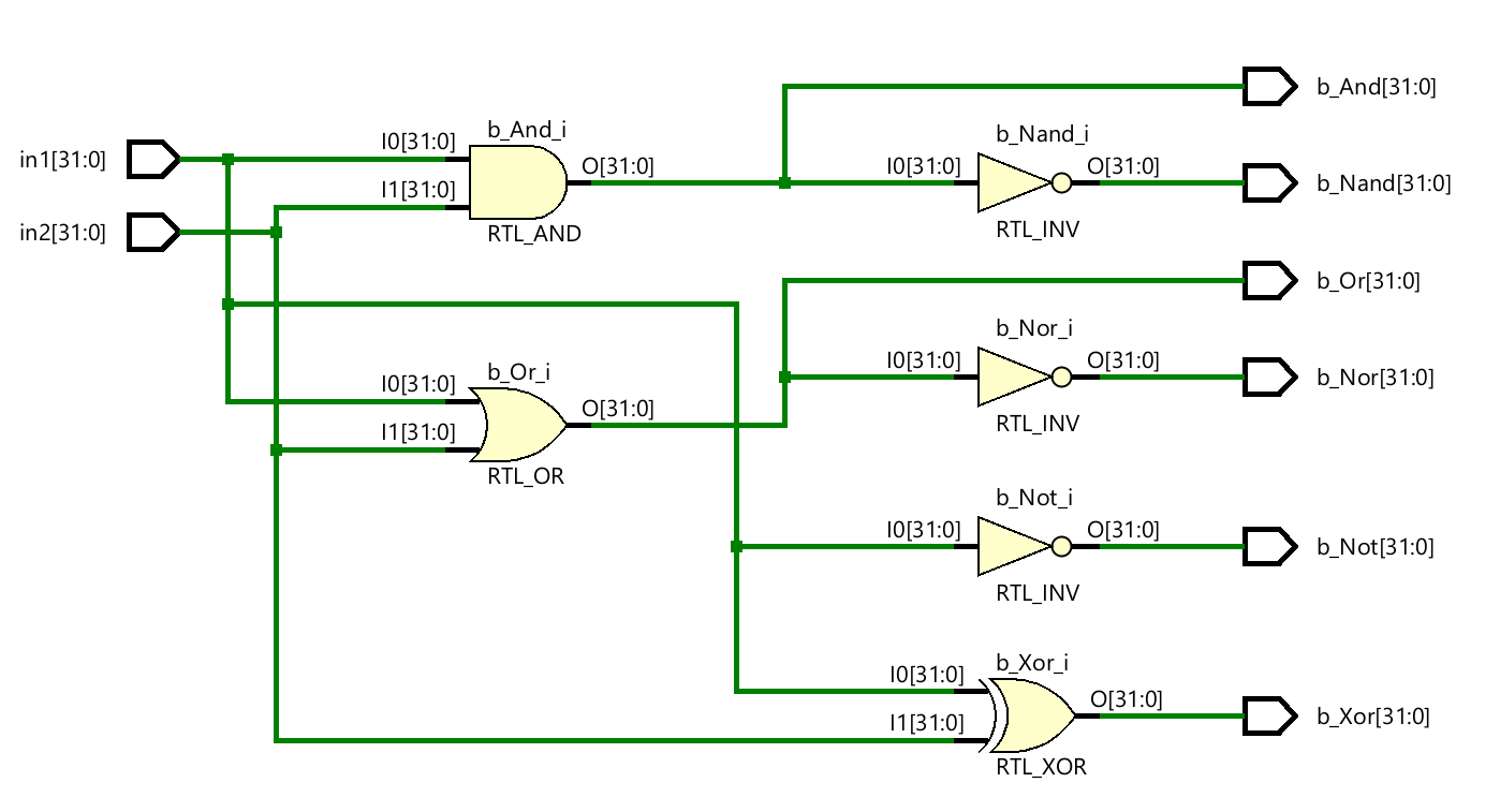 그림6 : multi bit RTL view 결과
1bit이든 multi-bit이든 상관없이 작성하시면 됩니다.
하지만 multi-bit인 상황에서는 logical operator이냐, bitwise operator이냐 에 따라 그 결과가 너무나도 다르게 나오므로...확실하게 알고 사용하시는 것이 중요합니다.
logical operator에서는 피연산자가 0이냐 아니냐에 따라 결과가 나오고 그 결과는 1bit으로 나옵니다.
만약 32bit vector 2개에 대한 bitwise연산을 하고 싶었지만 잘못해서 logical operator를 사용한다면 bitwise연산이 제대로 되지 않을 것입니다...
연산자가 이거외에도 너무나도 많고 그 연산자 간에 우선순위가 있으므로, 이 부분에 대해 추가로 공부하실 필요가 있긴합니다.
https://www.chipverify.com/verilog/verilog-operators
위 사이트에서 다양한 verilog syntax에 대해 다루고 있으니 한번 확인해보시면 좋겠습니다. 우선순위에 대한 내용은 다른 블로그에 정리된 것을 참고하길 바랍니다...
코너 속 코너에서 다루기엔 양이 많아서...흑흑
무튼 &,|,^,~을 사용해서 gate를 작성하면 RTL viewer로 본다면 해당 gate가 생성된 것을 볼 수 있다는 것을 보여드리고 싶었습니다.
(추가로 궁금하시면 이 부분에 대해 정리가 잘된 블로그들이 많으니...)
Two gates
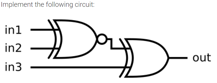 그림7 : Two gates
이번 문제에서는 위의 gate를 작성하라고 합니다.
바로 들어가보도록 합니다.
module top_module (
    input in1,
    input in2,
    input in3,
    output out);

    assign out = in3^~(in1^in2);

endmodule
이렇게 작성하면 됩니다!
More logic gate
위에서 다룬 내용이 문제로 나왔군요...
역시 HDLBits입니다..
다양한걸 해보라는 의도..
자 그럼 바로 문제로 들어가봅시다.
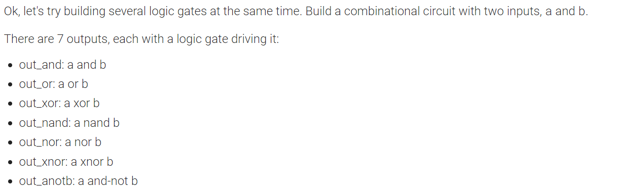 그림8 : More logic gate
module top_module(
    input a, b,
    output out_and,
    output out_or,
    output out_xor,
    output out_nand,
    output out_nor,
    output out_xnor,
    output out_anotb
);
    assign out_and = a&b;
    assign out_or = a|b;
    assign out_xor = a^b;
    assign out_nand = ~(a&b);
    assign out_nor = ~(a|b);
    assign out_xnor = ~(a^b);
    assign out_anotb = a&~b;

endmodule
네 이렇게 작성하시면 됩니다.
솔직히 여기까지는 너무 쉽지요?
7420 chip
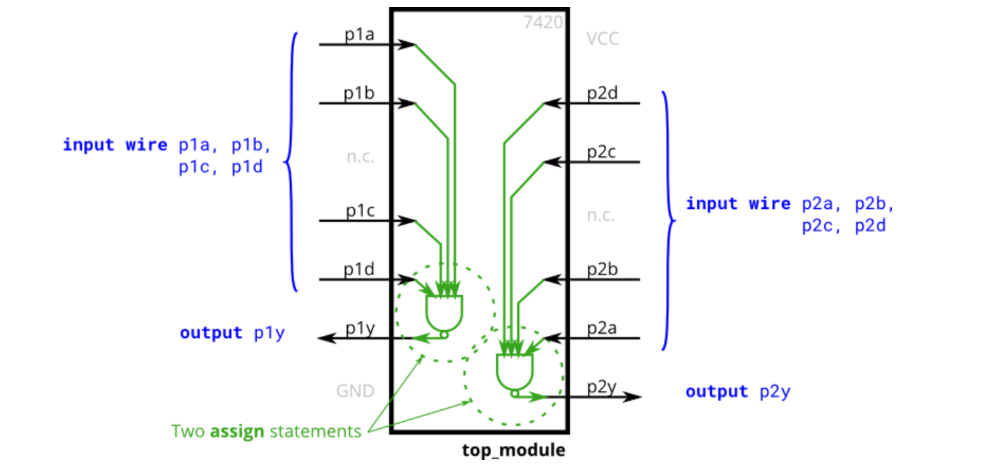 그림9 : 7420 chip
이번 문제는 7420 chip의 동작을 작성해보라고 합니다.
4input nand gate가 2개 있군요
그럼 바로 작성하러 가봅시다.
module top_module (
    input p1a, p1b, p1c, p1d,
    output p1y,
    input p2a, p2b, p2c, p2d,
    output p2y );


    assign p1y = ~(p1a&p1b&p1c&p1d);
    assign p2y = ~(p2a&p2b&p2c&p2d);

endmodule
Truth tables
이번에는 진리표를 보고 logic을 작성해보라고 하는군요.
이전에 combinational logic은 모든 입력, 출력에 대해 명확하게 정의되어야 한다고 했지요?
진리표가 그런걸 작성하는 표입니다.
입력이 3개이고 출력이 1개인경우 8개의 입력에 대해 출력을 작성해주어야 합니다.
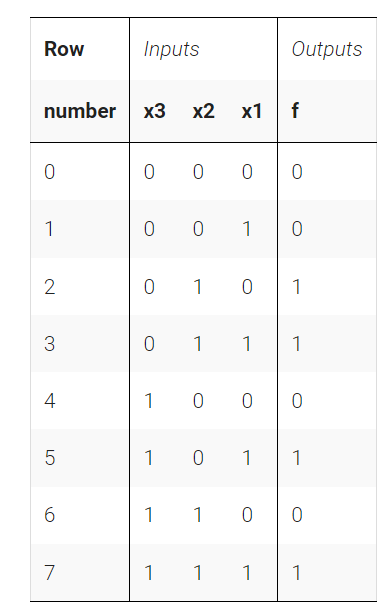 그림10 : Truth tables
위의 그림처럼 진리표를 작성했다면 이를 어떻게 logic gate로 기술하느냐?
출력이 1인 경우에 대해 sum of product형식으로 작성하면 됩니다.
조금 더 구체적으로 말씀드리자면, 출력이 1이 되는 것이 지금 2,3,5,7행이 있습니다.
여기에 대해 and or gate로 작성하면 된다는 것입니다.
2번행이 되기 위해서는 x3=0,x2=1,x1=0이 동시에 만족해야겠지요?
나머지 3,5,7행에 대해서도 동일하게 만족해야하는 조건이 있지요?
그건 and gate로 엮어주시면 됩니다.
여러조건이 동시에 만족해야하니까요
그렇다면 출력이 1이 되기 위해서는 2,3,5,7행 중 하나라도 만족하면 1이 되잖아요?
그래서 그런 경우에는 or gate로 엮어주면 됩니다.
여기까지 따라왔다면 문제로 들어가봅시다.
module top_module(
    input x3,
    input x2,
    input x1,  // three inputs
    output f   // one output
);

    assign f = (~x3&x2&~x1)|(~x3&x2&x1)|(x3&~x2&x1)|(x3&x2&x1);


endmodule
Two-bot equality
이번 문제에서는 비교기에서 등호를 만들어봐라는 문제입니다.
이건 if-else,case,삼항 연산자 등 여러가지 선택지가 있겠지요?
선택은 자유입니다
저는 간단하게 삼항 연산자로 하도록 하겠습니다.
module top_module ( input [1:0] A, input [1:0] B, output z );

    assign z = A==B ? 1'b1:1'b0;
endmodule
Simple circuit A
module top_module (input x, input y, output z);
    assign z = (x^y)&x;
endmodule
이건 문제로 왜 있는지 모르겠군요 정답이 문제 상단에 나와있습니다...
Simple circuit B
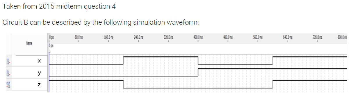 그림11 : Simple circuit B
위의 waveform을 보고 이런 동작을 하는 circuit을 작성해보라는 겁니다.
??? 왜 갑자기 waveform이죠? 어려운 거 없습니다.
그냥 진리표를 제공해주었구나 생각하시면 되겠습니다.
정말로 간단하게 xor에 not을 붙인 녀석이라는 것을 알 수 있습니다.
이렇게 바로 보지 못하여도, z = (x&~y)|(~x&y); 이런식으로 작성해주어도 됩니다.
module top_module ( input x, input y, output z );

    assign z = ~(x^y);

endmodule
Combine circuits A and B
위의 Simple circuit A,B를 합치라고 하는 문제입니다.
합치고 나서 그걸 바로 출력으로 보내는 것이 아니라 이 후 간단한 logic gate를 통과시킨 걸 출력으로 보내라는 문제입니다.
이건에 Modules편에서 인스턴스 생성하고 작성하는 방법에 다루었으니, 바로 문제도 들어가봅시다.
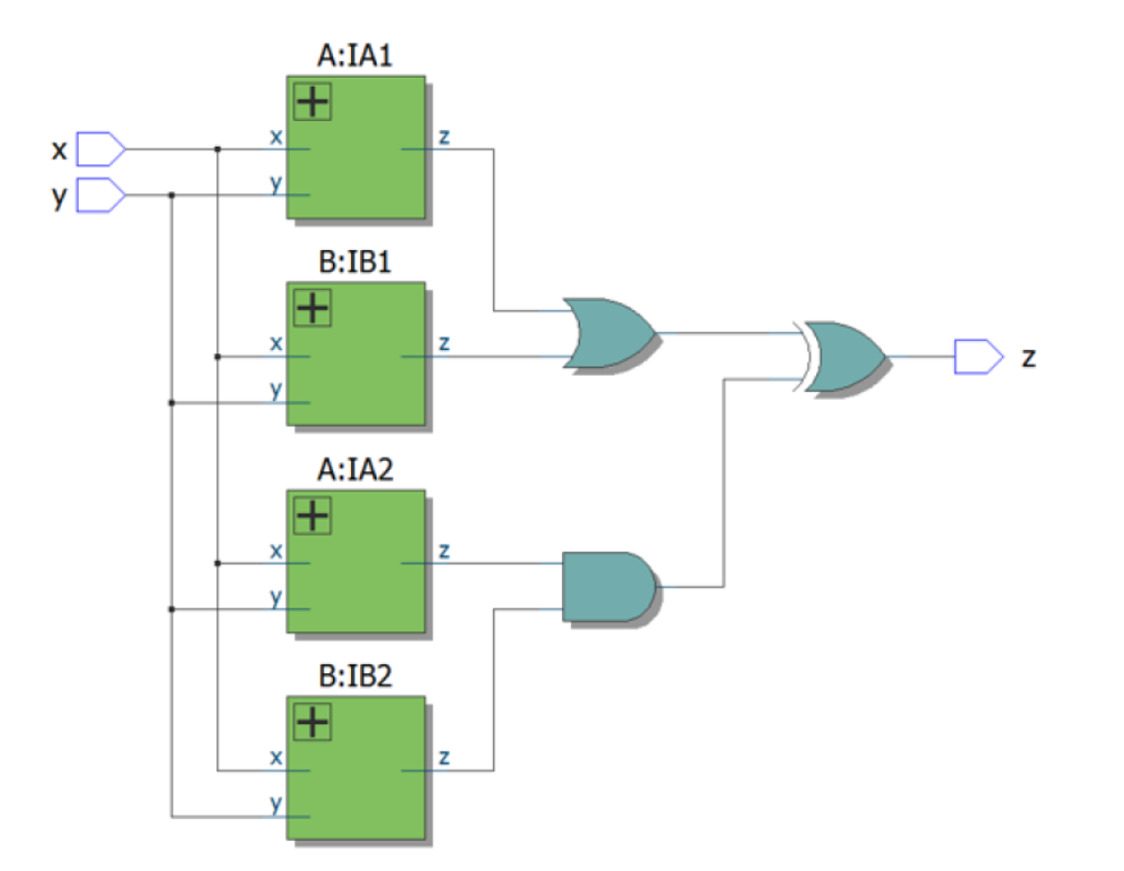 그림12 : Combine circuits A and B
`default_nettype none
module top_module (input x, input y, output z);

    wire z1,z2,z3,z4;

    A IA1(
        .x(x),
        .y(y),
        .z(z1)
    );

    A IA2(
        .x(x),
        .y(y),
        .z(z2)
    );

    B IB1(
        .x(x),
        .y(y),
        .z(z3)
    );

    B IB2(
        .x(x),
        .y(y),
        .z(z4)
    );


    assign z = (z1|z2)^(z3&z4);


endmodule


module A (input x, input y, output z);
    assign z = (x^y)&x;
endmodule

module B ( input x, input y, output z );

    assign z = ~(x^y);

endmodule
이렇게 아래에 위에서 했던 A,B를 작성해주시고 top module을 작성하면 되겠습니다.
Ringer
이번 문제는 ringer를 만들라고 하는 군요.
사실 이건 중요하지 않습니다.
문제의 핵심은 현재 설명이 SW 프로그래밍에 적합하게 되어있다는 것인데, 이걸 어떻게 assign 해서 HW적으로 작성할 것이냐를 보는 것입니다.
보통 우리가 순차적인 내용을 작성할 때, 입력이 이러면 출력은 이렇다 라고 작성을 하지요 하지만 반대로도 생각해보면 좋다는 것을 알려주기 위한 문제 같습니다.
출력이 이렇게 되기 위해서는 입력은 어떻게 되어야 하는가에 대해서도 생각해보라는 문제입니다.
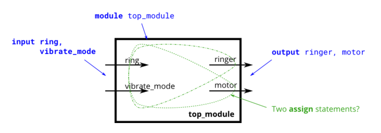
module top_module (
    input ring,
    input vibrate_mode,
    output ringer,       // Make sound
    output motor         // Vibrate
);

    assign ringer = vibrate_mode ? 0:ring;
    assign motor = vibrate_mode ? ring:0;

endmodule
module top_module(
input ring,
input vibrate_mode,
output ringer,
output motor
);
// When should ringer be on? When (phone is ringing) and (phone is not in vibrate mode)
assign ringer = ring & ~vibrate_mode;
// When should motor be on? When (phone is ringing) and (phone is in vibrate mode)
assign motor = ring & vibrate_mode;
endmodule위의 코드처럼 작성하면 됩니다.
위에서 assign으로 해결하는 것은 먼저 출력이 이렇게 되기 위해서는 입력이 어떻게 되어야 하는가를 고민하지요?
반면 SW프로그래밍을 할 때는 입력이 이런 경우? 출력은 이렇다인데, 뭔가 flow가 반대이지요? 때로는 HDL을 기술할 때 출력에 대해 입력조건을 생각해보는 것이 도움이 많이 된다는 것을 알고 넘어가라는 문제인듯합니다.
그래서 이게 아니라면 always block을 사용하면 조금더 SW프로그래밍적?으로 작성할 수는 있겠지요.
Thermostat
이번에는 heating/cooling thermostat에 대한 문제이군요.
그 logic에 대해 읽어보고 작성해보면 되겠습니다.
mode = 1이면 heating이고 mode = 0이면 cooling이라고 하는군요.
그리고 too_cold = 1이면 heater를 틀고, air conditioner를 끄라고 하는 군요.
그 반대로 too_hot이면 위의 반대로 하라고 하는군요.
그리고 fan은 heater와 air conditioner가 켜지면 틀라고 하고 따로 fan을 킬 수 있는 logic을 추가하라는 군요.
문제를 쭉 읽다보니 좀 복잡해보이는데, fan, aircon, heater에 대해 생각해봅시다.
그리고 assign statement를 사용해서 작성하라고 하는군요.
그럼 바로 문제로 들어가봅시다.
module top_module (
    input too_cold,
    input too_hot,
    input mode,
    input fan_on,
    output heater,
    output aircon,
    output fan
);
    assign heater = (mode==1) ? (too_cold) ? 1 : 0 : 0;
    assign aircon = (mode==0) ? (too_hot) ? 1 : 0 : 0;
    assign fan = heater | aircon | fan_on;

endmodule
우선 heater와 aircon에 대해 먼저 작성해주었습니다.
fan은 heater,aircon,fan_on의 영향을 받기에 나중에 작성해주었습니다.
그렇게 하지 않으면 fan도 입력에 대해 combinational logic을 작성해줘야겠지요?
이렇게 하면 assign해둔 output을 이용해서 간단하게 fan에 대한 logic을 작성할 수 있습니다.
module top_module(
	input too_cold,
	input too_hot,
	input mode,
	input fan_on,
	output heater,
	output aircon,
	output fan
);
	// Reminder: The order in which you write assign statements doesn't matter.
	// assign statements describe circuits, so you get the same circuit in the end
	// regardless of which portion you describe first.

	// Fan should be on when either heater or aircon is on, and also when requested to do so (fan_on = 1).
	assign fan = heater | aircon | fan_on;

	// Heater is on when it's too cold and mode is "heating".
	assign heater = (mode & too_cold);

	// Aircon is on when it's too hot and mode is not "heating".
	assign aircon = (~mode & too_hot);

	// * Unlike real thermostats, there is no "off" mode here.

endmodule
솔루션에는 이렇게 작성되어있군요. 이게 좀 더 좋아보입니다.
왜냐하면 제가 작성한 답은 mux를 사용하고 mux 자체가 여러개의 gate로 이루어져있기에 logic gate를 조금 더 사용하는 것이라 볼 수 있겠습니다.
하지만 간단하게 and, or로 작성할 수 있는 경우, 위의 솔루션처럼 하는 것이 좋아보입니다.
(오히려 제가 짠거 보다 직관적이기도 하군요)
3-bit population count
population count circuit을 작성해보라고 합니다.
이전에도 몇번 해봤지요?
그 때는 for문을 이용해서 작성해었던 것으로 기억합니다.
1의 개수를 세는 문제입니다.
module top_module(
    input [2:0] in,
    output [1:0] out );

    assign out = in[2] + in[1] + in[0];

endmodule
이렇게 해도 되고 아니면 진리표를 작성해서 기술해도 됩니다만, 저는 이렇게 하는게 편한 것 같습니다.
Gates and vectors
bit간 관계에 대해 구하는 circuit을 작성하라고 합니다.
module top_module(
    input [3:0] in,
    output [2:0] out_both,
    output [3:1] out_any,
    output [3:0] out_different );

    assign out_both = {in[3]&in[2],in[2]&in[1],in[1]&in[0]};
    assign out_any = {in[3]|in[2],in[2]|in[1],in[1]|in[0]};
    assign out_different = {in[0]^in[3],in[3]^in[2],in[2]^in[1],in[1]^in[0]};

endmodule
이렇게 해도 되지만 솔루션이 좀 더 좋은 표현인듯 합니다.
module top_module (
	input [3:0] in,
	output [2:0] out_both,
	output [3:1] out_any,
	output [3:0] out_different
);

	// Use bitwise operators and part-select to do the entire calculation in one line of code
	// in[3:1] is this vector:   					 in[3]  in[2]  in[1]
	// in[2:0] is this vector:   					 in[2]  in[1]  in[0]
	// Bitwise-OR produces a 3 bit vector.			   |      |      |
	// Assign this 3-bit result to out_any[3:1]:	o_a[3] o_a[2] o_a[1]

	// Thus, each output bit is the OR of the input bit and its neighbour to the right:
	// e.g., out_any[1] = in[1] | in[0];
	// Notice how this works even for long vectors.
	assign out_any = in[3:1] | in[2:0];

	assign out_both = in[2:0] & in[3:1];

	// XOR 'in' with a vector that is 'in' rotated to the right by 1 position: {in[0], in[3:1]}
	// The rotation is accomplished by using part selects[] and the concatenation operator{}.
	assign out_different = in ^ {in[0], in[3:1]};

endmodule
Even longer vectors
위의 문제에서 한 것을 조금 더 긴 vector에 대해 적용해봐라 는 문제입니다.
바로 들어가보죠
module top_module(
   input [99:0] in,
   output [98:0] out_both,
   output [99:1] out_any,
   output [99:0] out_different );

   assign out_both = in[98:0]&in[99:1];
   assign out_any = in[98:0]|in[99:1];
   assign out_different = in^{in[0],in[99:1]};

endmodule
어때요 쉽나요?
조금 힘들어다면 먼저 한번 bit 그림을 그려서 그 생각해보는 것을 추천합니다.
자 여기까지가 combinational logic의 Basic gates내용들이었습니다.
다음편에서는 Mux에 대한 내용으로 돌아오겠습니다!