Storage Technologies
if you understand how the system moves data up and down the memory hierarchy, then you can write your application programs so that their data items are stored higher in the hierarchy, where the CPU can access them more quickly.
시스템이 어떻게 데이터를 메모리 계층구조에서 움직이는지 이해한다면, 메모리 상위 계층에 데이터가 저장되는 프로그램을 짤 수 있습니다. 따라서 CPU는 더 빨리 데이터에 접근이 가능합니다!
This idea centers around a fundamental property of computer programs known as locality. Programs with good locality tend to access the same set of data items over and over again, or they tend to access sets of nearby data items. Programs with good locality tend to access more data items from the upper levels of the memory hierarchy than programs with poor locality, and thus run faster. For example, on our Core i7 system, the running times of different matrix multiplication kernels that perform the same number of arithmetic operations, but have different degrees of locality, can vary by a factor of almost 40!
해당 아이디어는 '지역성' 이라고 알려진 컴퓨터 프로그램의 근본 특성에 중심을 둔다. 지역성 좋은 프로그램은 같은 set의 데이터들을 계속해서 접근하거나, 그 근처에 있는 데이터로 접근하는 경향을 보입니다.
좋은 지역성을 갖는 프로그램은 메모리 상위 계층의 레벨에 있는 데이터에 더 자주 접근합니다.
SRAM
SRAM stores each bit in a bistable memory cell. Each cell is implemented with a six-transistor circuit. This circuit has the property that it can stay indefinitely in either of two different voltage configurations, or states. Any other state will be unstable—starting from there, the circuit will quickly move toward one of the stable states. Such a memory cell is analogous to the inverted pendulum illustrated in Figure 6.1.
역진자가 어쩌고 저쩌고... 뭔소리야..!!! 이 부분은 넘어가기로 하고 SRAM이 왜 DRAM 보다 빠른지만 요약해보았다!!
- Access Speed (액세스 속도): SRAM은 데이터에 액세스하기 위해 캐패시터 충전 및 방전과 같은 복잡한 프로세스를 거치지 않습니다. 대신에 SRAM은 간단한 논리 게이트 및 플립플롭으로 구성되어 있어 데이터에 더 빠르게 액세스할 수 있습니다.
- Refresh Cycle (새로고침 주기): DRAM은 주기적인 새로고침이 필요합니다. 이는 캐패시터의 충전 상태가 시간이 지나면 약해져서 데이터를 잃을 수 있기 때문입니다. 하지만 SRAM은 새로고침이 필요하지 않습니다. 따라서 SRAM은 데이터에 대한 액세스를 위해 추가적인 시간을 소비하지 않아도 되므로 더 빠릅니다.
- 구조적 차이: SRAM은 플립플롭을 사용하여 각 비트를 저장하는 반면, DRAM은 캐패시터와 트랜지스터로 구성된 복잡한 회로를 사용합니다. SRAM의 간단한 구조는 데이터에 대한 액세스를 더 빠르게 만듭니다.
DRAM
DRAM stores each bit as charge on a capacitor. This capacitor is very small-typically around 30 femtofarads—that is, 30 × 10-15 farads. Recall, however, that a farad is a very large unit of measure. DRAM storage can be made very dense— each cell consists of a capacitor and a single access transistor. Unlike SRAM, however, a DRAM memory cell is very sensitive to any disturbance. When the capacitor voltage is disturbed, it will never recover. Exposure to light rays will cause the capacitor voltages to change. In fact, the sensors in digital cameras and camcorders are essentially arrays of DRAM cells.
패러드(Farad)는 전기 용량을 측정하는 단위입니다. 이것이 "매우 큰 단위"라고 설명된 것은, 대부분의 전기 용량 측정에서 일반적으로 사용되는 단위가 마이크로패러드(Microfarad, 10^-6 패러드) 또는 나노패러드(Nanofarad, 10^-9 패러드) 수준이기 때문입니다. 따라서 패러드는 이러한 일반적인 단위보다 훨씬 큰 값으로 사용됩니다.
DRAM은 각각의 비트를 캐퍼시터에 저장합니다. DRAM은 매우 밀집되어 제작될 수 있으며 각각의 셀은 캐퍼시터와 접근 트랜지스터로 구성됩니다. SRAM과는 달리 DRAM은 작은 방해(?)에도 매우 민감하게 반응합니다. 캐퍼시터의 전압이 다운되면, 절대 복구가 되지 않습니다. 빛을 캐퍼시터에 쬐게하면 전압이 변할 수 있습니다.
Conventional DRAMs
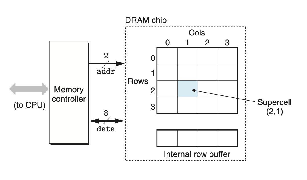
The cells (bits) in a DRAM chip are partitioned into d supercells, each consisting of w DRAM cells. A d × w DRAM stores a total of dw bits of information. The supercells are organized as a rectangular array with r rows and c columns, where rc = d. Each supercell has an address of the form (i, j), where i denotes the row and j denotes the column.
DRAM은 i,j의 2차원 배열로 이루어져 있으며 혼란을 피하기 위해 이 책에서는 i,j에 대응 되는 셀을 SuperCell 이라고 부르겠습니다!
For example, Figure 6.3 shows the organization of a 16 × 8 DRAM chip with d = 16 supercells, w = 8 bits per supercell, r = 4 rows, and c = 4 columns. The shaded box denotes the supercell at address (2, 1). Information flows in and out of the chip via external connectors called pins. Each pin carries a 1-bit signal. Figure 6.3 shows two of these sets of pins: eight data pins that can transfer 1 byte in or out of the chip, and two addr pins that carry two-bit row and column supercell addresses. Other pins that carry control information are not shown.
비트 정보는 핀(pin) 이라 불리는 외부 커넥터에 의해 칩과 메모리 사이를 이동합니다. 각각의 핀은 1비트 정보를 옮길 수 있습니다. 그림에서는 8개의 데이터 핀을 나타냅니다.
Each DRAM chip is connected to some circuitry, known as the memory controller, that can transfer w bits at a time to and from each DRAM chip. To read the contents of supercell (i, j ), the memory controller sends the row address i to the DRAM, followed by the column address j . The DRAM responds by sending the contents of supercell (i, j ) back to the controller. The row address i is called a RAS (row access strobe) request. The column address j is called a CAS (column access strobe) request. Notice that the RAS and CAS requests share the same DRAM address pins.
DRAM 칩은 각각의 DRAM 칩들로부터 비트 정보를 전송할 수 있는 Memory Controller와 연결되어 있습니다. 슈퍼셀(i,j)로부터 정보를 읽으려면, 메모리 컨트롤러는 행 주소 i를 DRAM에 보내고, 다음에 열 주소 j를 DRAM에 보냅니다.
행 주소 i 는 RAS (Row Access Strobe) 라 불리고
열 주소 j 는 CAS (Column Access Strob)라 불립니다.
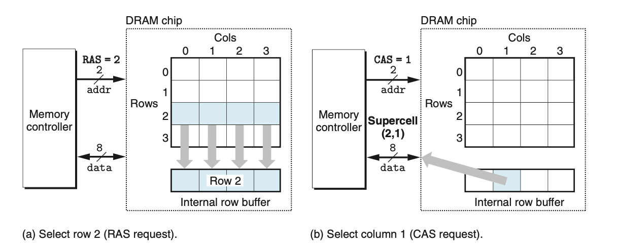
For example, to read supercell (2, 1) from the 16 × 8 DRAM in Figure 6.3, the memory controller sends row address 2, as shown in Figure 6.4(a). The DRAM responds by copying the entire contents of row 2 into an internal row buffer. Next, the memory controller sends column address 1, as shown in Figure 6.4(b). The DRAM responds by copying the 8 bits in supercell (2, 1) from the row buffer and sending them to the memory controller.
예를 들어서 , 슈퍼셀 (2,1)을 읽으려면,
1. 메모리 컨트롤러는 Row 주소2를 보냅니다. (RAS Request)
2. DRAM은 내부 로우 버퍼에 row2의 전체 내용을 복사합니다.
3. 그 다음, 메모리 컨트롤러는 col1 주소를 보냅니다. (CAS Request)
4. DRAM은 행 버퍼에서 슈퍼셀(2,1)에 있는 8비트를 복사해서 메모리 컨트롤러에 보냅니다.
One reason circuit designers organize DRAMs as two-dimensional arrays instead of linear arrays is to reduce the number of address pins on the chip. For example, if our example 128-bit DRAM were organized as a linear array of 16 supercells with addresses 0 to 15, then the chip would need four address pins instead of two. The disadvantage of the two-dimensional array organization is that addresses must be sent in two distinct steps, which increases the access time.
128 비트 (27)를 8로 나누면 16이다. 즉, 선형적 늘어진 16개를 구분하기 위해서는 4개의 주소 핀 (24 = 16)이 필요하게 되는 것이다!
즉, DRAM 구조는 메모리 핀 주소의 갯수와 접근 타임에 대한 트레이드 오프를 고려하여 설계된 것이다.
Nonvolatile Memory
ROMs
DRAMs and SRAMs are volatile in the sense that they lose their information if the supply voltage is turned off. Nonvolatile memories, on the other hand, retain their information even when they are powered off. There are a variety of nonvolatile memories. For historical reasons, they are referred to collectively as read-only memories (ROMs), even though some types of ROMs can be written to as well as read. ROMs are distinguished by the number of times they can be reprogrammed (written to) and by the mechanism for reprogramming them.
DRAM, SRAM 모두 전원이 꺼지면 정보를 잃기 때문에 휘발성이다. 하지만 비휘발성 메모리는 그렇지 않다.
ROM(Read Only Memory)는 쓰기가 되지만, 역사적인 이유로 ROMs 이라고 부르겠습니다!
ROMs 은 재프로그램(쓰기)의 횟수에 따라서, 방법에 따라 구분됩니다.Erasable Programmable ROM
An erasable programmable ROM (EPROM) has a transparent quartz window that permits light to reach the storage cells. The EPROM cells are cleared to zeros by shining ultraviolet light through the window. Programming an EPROM is done by using a special device to write ones into the EPROM. An EPROM can be erased and reprogrammed on the order of 1,000 times. An electrically erasable PROM (EEPROM) is akin to an EPROM, but it does not require a physically separate programming device, and thus can be reprogrammed in-place on printed circuit cards. An EEPROM can be reprogrammed on the order of 105 times before it wears out.
EPROM은 빛이 저장장치 셀에 도달할 수 있는 투명한 수정 윈도우를 갖고있다. EPROM 셀은 이 투명한 수정 윈도우를 통해 자외선을 비추면 0으로 지울 수 있다. EPROM을 프로그래밍 하는 것은 EPROM에 1을 쓸 수 있는 특별한 장치를 사용해서 이루어진다.
Electrically erasable PROM (EPROM)은 물리적으로 별도의 프로그램 장치를 필요로 하지 않고, PCB에서 직접 재프로그램 될 수 있다.
Flash memory
Flash memory is a type of nonvolatile memory, based on EEPROMs, that has become an important storage technology. Flash memories are everywhere, providing fast and durable nonvolatile storage for a slew of electronic devices, including digital cameras, cell phones, and music players, as well as laptop, desktop, and server computer systems. In Section 6.1.3, we will look in detail at a new form of flash-based disk drive, known as a solid state disk (SSD), that provides a faster, sturdier, and less power-hungry alternative to conventional rotating disks.
플래시 메모리는 EEPROMs를 기반으로 한 비 휘발성 메모리의 한 종류로, 중요한 저장장치 기술이 됐습니다. 디지털 카메라, 휴대폰, 노트북, 데스크탑과 서버 컴퓨터 시스템 등 어디에서나 플래시 메모리를 찾을 수 있습니다.
Accessing Main Memory
Data flows back and forth between the processor and the DRAM main memory over shared electrical conduits called buses. Each transfer of data between the CPU and memory is accomplished with a series of steps called a bus transaction. A read transaction transfers data from the main memory to the CPU. A write transaction transfers data from the CPU to the main memory.
프로세서와 DRAM간의 데이터 이동은 BUS라고 불리는 전선에서 Bus Transaction을 통해서 이뤄집니다.
Read : DRAM -> Processor
write : Processor -> DRAM
A bus is a collection of parallel wires that carry address, data, and control signals. Depending on the particular bus design, data and address signals can share the same set of wires or can use different sets. Also, more than two devices can share the same bus. The control wires carry signals that synchronize the transaction and identify what kind of transaction is currently being performed. For example, is this transaction of interest to the main memory, or to some other I/O device such as a disk controller? Is the transaction a read or a write? Is the information on the bus an address or a data item?
버스는 주소, 데이터, 제어신호들을 운반하는 전선의 병렬 배치 입니다. 버스를 어떻게 설계하는지에 따라서 데이터와 주소 신호들은 같은 전선을 사용하거나, 다른 전선을 사용하게 됩니다.
또한, 2개 이상의 기기에서 같은 버스를 공유할 수 있습니다.
제어선들은 트랜잭션을 동기화하는 신호들을 운반하고, 어떤 트랙잭션이 현재 수행중인지 확인합니다.
예를 들어서, (signals from control wires)
해당 트랜잭션이 메인 메모리로 가는지, 아니면 disk contoller와 같은 I/O 디바이스인지? 혹은 read, write 인지? 혹은 주소인지 데이터 그 자체인지를 판별합니다.
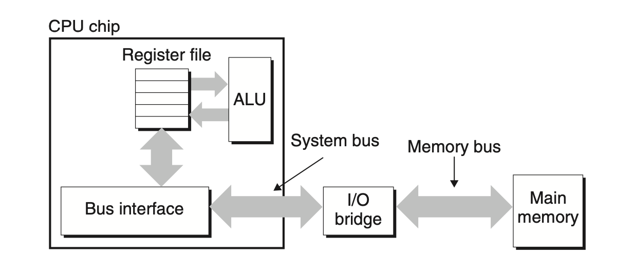
It shows the configuration of an example computer system. The main components are the CPU chip, a chipset that we will call an I/O bridge (which includes the memory controller), and the DRAM memory modules that make up main memory. These components are connected by a pair of buses: a system bus that connects the CPU to the I/O bridge, and a memory bus that connects the I/O
CPU, I/O bridge(Memory Controller를 포함) 그리고 DRAM 메인 메모리 모듈이 주요 컴포넌트이다.
System bus : CPU와 I/O bridge를 연결하는 시스템 버스.
memory bus : I/O와 메인 메모리를 연결하는 메모리 버스.
The I/O bridge translates the electrical signals of the system bus into the electrical signals of the memory bus. As we will see, the I/O bridge also connects the system bus and memory bus to an I/O bus that is shared by I/O devices such as disks and graphics cards. For now, though, we will focus on the memory bus.
I/O 브릿지는 시스템버스의 전기적 신호를 메모리 버스의 전기적 신호로 번역해줍니다. I/O 브릿지는 시스템 버스와 메모리 버스를 디스크나 그래픽 카드 같은 입출력 장치들이 공유하는 I/O 버스로 연결한다.
Consider what happens when the CPU performs a load operation such as
movq A,%raxwhere the contents of address A are loaded into register %rax. Circuitry on the CPU chip called the bus interface initiates a read transaction on the bus. The read transaction consists of three steps. First, the CPU places the address A on the system bus. The I/O bridge passes the signal along to the memory bus (Figure 6.7(a)). Next, the main memory senses the address signal on the memory bus, reads the address from the memory bus, fetches the data from the DRAM, and writes the data to the memory bus. The I/O bridge translates the memory bus signal into a system bus signal and passes it along to the system bus (Figure 6.7(b)). Finally, the CPU senses the data on the system bus, reads the data from the bus, and copies the data to register %rax (Figure 6.7(c)).
CPU가 아래의 load operation을 수행하는 상황을 가정해봅시다.
movq A,%rax
**프로세서는 Bus Interface를 호출하여 Read Transaction을 버스에 시행합니다.** 1. I/O bridge는 시그널을 메모리 버스로 보냅니다. 2. 메인 메모리는 address signal을 memory bus를 통해 감지합니다, memory bus로부터 address를 읽고 DRAM으로부터 데이터를 가져온 뒤 메모리 버스에 데이터를 write 합니다. 3.I/O bridge는 memory bus signal을 system bus signal로 번역 후 패스해줍니다. 4. 마지막으로, CPU는 system bus로부터 데이터를 감지하고, 버스로부터 데이터를 읽은 뒤 register %rax에 데이터를 카피합니다.
