
2.1 overview
Application Engineer 가 칩 선정시 고려해야 할 점.
1.어떤 Cortex-M Processor 가 니즈에 가장 취합하는 지?
2.얼마만큼의 메모리가 필요한지?
3.얼마큼 빠른게 시스템이 운영되야 하는지(Clock Speed)?
4.어떤 Peripherals 들이 필요한지?
ASIC 디자인을 위해서는 다양한 고려사항들이 존재합니다. 일반적인 칩 디자인 고려사항으로는 다음과 같은 것들이 있습니다:
1.어떤 반도체 공정 노드를 사용할 것인가?
2.어떤 유형의 메모리 기술이 사용 가능한가? (예: 소형 기하학 프로세스 노드에는 내장형 플래시 메모리가 제공되지 않음)
3.비휘발성 메모리(NVM) 프로그래밍은 어떻게 처리해야 하는가?
4.어떤 종류의 전력 관리 기능을 사용해야 하는가?
5.어떤 종류의 칩 패키징을 사용해야 하는가?
6.장치 제조 테스트를 위해 필요한 디자인-포-테스트(DFT) 기능은 무엇인가?
7.IoT 시대에서는 보안 측면 및 다른 다양한 도전적인 영역에서 무선 통신 인터페이스를 SoC 디자인에 통합하는 것도 고려해야 합니다.
이 문서에서는 프로세서 시스템 디자인 영역에 대해서만 살펴보도록 하겠습니다. 간단한 Cortex-M 프로세서 시스템을 작동시키기 위해서는 보통 다음과 같은 사항을 고려해야 합니다
1.메모리 블록 - 어떤 종류의 메모리가 필요하고, 어떤 크기의 메모리가 필요한가?
2.페리페럴 - 어떤 페리페럴이 필요하고, 필요한 경우 페리페럴을 만드는 것?
3.클럭 및 리셋 스킴 - 클럭 신호를 생성하고 분배하는 방법, 전원 상태 및 리셋 조건 처리 방법?
4.인터럽트 처리 - 다양한 소스에서 발생하는 인터럽트를 어떻게 우선순위를 두고 처리할 것인가?
5.버스 아키텍처 - 서로 다른 블록을 어떻게 연결하고 어떤 버스 프로토콜을 사용할 것인가?
6.전력 관리 - 작동 및 저전력 모드에서 전력 소비를 어떻게 줄일 것인가?
7.디버깅 및 추적 - 개발 및 테스트 중 디버깅 및 추적 기능을 제공하는 방법?
8.Event Interface integration.
2.2 What memories are needed?
2.2.1 Overview of memories
In a typical Cortex-M based system, there are at least two types of memories:
Non-volatile memory(NVM), typically using embedded flash technologies or masked ROM, for program storage:
RAM, for read-write data including stack and heap.
특정 시스템에는 추가적인 메모리가 있을 수 있음. For Boot loader and Ohter preloaded firmware.
Some low-power devices also have special retention static RAM(SRAM) for holding small amounts of data while the reset of the device is shut down during sleep modes. -> sleep mode 에서 데이터 유지됨.
대부분의 M Processors 는 32bit AHB 를 사용하고, 그러므로 메모리 시스템은 32 bit wide 로 설계 되어야 한다. 그러나 반드시 byte adressable 할 필요는 있다. 이것은 RAM 이 반드시 byte(8-bit),half-word(16-bit) and word(32-bit) write operations 을 제공해야 한다는 것이다.
FPGA Base인 Project 에서는
FPGA 안의 SRAM 은 프로그램 저장소(Most FPGA Initialization Sequences can initialize SRAM contents at the same time)와 Read-Write Data 로 사용 될수 있다.
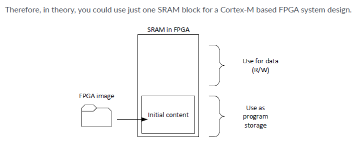
However, Such an arragement differs from ASIC/SoC system designs where SRAM cannot be initialized in the same way. Also, doing so will impack performance on a Cortex-M3/M4-based system as it will no longer be using a Harvard bus architecture. To avoid confusion. the rest of the examples in this book use two memory blocks for separation program storage and data read-writes.
2.2.2 Memory declarations in FPGA design tools
If you are using FPGA DesignStart, the memory system for the Cortex-M1 or Cortex-M3 could be generated for you by the FPGA design tools, so it is easy to do. However, if you are not using FPGA DesignStart, you might need to handle the memory integration manually.
A long time ago, FPGA tools could not generate RAM blocks using behavioral Verilog codes and declaration of memories in FPGA projects required instantiation of memory macros manually. This was changed a few years ago, bu such a capabuility might require the RAM declarations to be wriiten in a specific way to allow the FPGA design tools to recignize it correctly.
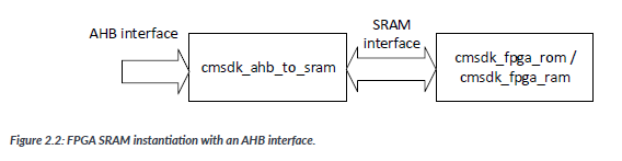
This arragement allows you to swap over the FPGA ROM/ RAM with other memories easily(e.g., when migrating to ASIC)
2.2.3 Memory handling in ASIC designs
In ASIC desgin, SRAM and NVM blocks cannot be generated from verilog RTL in behavioral synthesis. Typically, you need a specific memory generation tool(SRAM compiler) to create the SRAM, and for embedded flash, you need to instantiate the flash macro manually.
2.2.4 Memory endianness
When designing memory systems, one of the considerations is endianness. Most Cortex-M systems today are based on little-endian memory system. However, it is possible to create big-endian Cortex-M systems as there processors support big-endian configuration options. When doing this it is important to make sure that the software developers of the product are aware so that they can use correct comilation switched in their software projects.
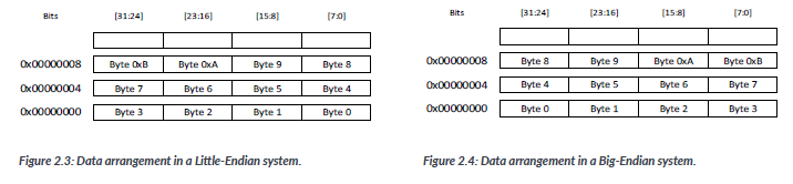
Please note that the endiann configuration only affect data accesses(including read-noly data). instructions are always encoding as little endian. Also, access to the Private Peripheral Bus is alwaysin little endian.
2.3 Defining the Peripherals
A microcontroller is not complete without range of peripherals for variou input/output and hardware control functions such as timers. For the most basic Cortex-M based systems, we would expect to find digital peripherals like :
General-Purpose input/output (GPIO) :
Timers :
Pulse Width Modulator(PWM) - usually for motor or power electronic system control;
UART for serial communication;
SPI(Serial Periheral Interface);
I2C/I3C - commonly used for sensors.
In addition to these basic peripherals, a simple system might also integrate a group of registers for various system control functions (e.g. clock source control, selection of low-power modes). This coulld be integrated as part of the peripheral system, but additinal care must be taken for system security reasons. Typically, system management functions need to be restricted to privilege accesses only.
2.4 Memory map definition
The architectures used in the cortex-M processors define a memory map that allocates address ranges into regions. This allows the built-in peripherals like the interrupt controller and debug components to be accessed by simple memory access instructions, thus allowing system features to be accessible in C program code.
Having a predefined memory map also allows the Cortex-M processors to be optimized for performance. For example, a memory region called CODE at the beginning of be optimized for performance. For example, a memory region called CODE at the beginning of the memory is dedicated to program memory, and a memory region called SRAM starting from 0x2000000 is dedicated to data memory. In the Cortex-M3 processor, CODE and SRAM regions use separated bused to allow the system to utilize the performance benefits of a HAVARD bus arhitecture. it is possible to use the memory regions differently, but it may not be able to get the best performace by doing so.
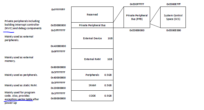
The top 512Mb of the System Level Memory contains a region for system control and reserved areas.
This bus provides access to the built-in interrupt controller and various debug componets. Within the PPB range, a special range of memory is defined as System Control Space(SCS). it contains the interrupt control, it contains the interrupt control registers, system control register, debug control registers, and so on. The remaining system-level memory space from address 0xE0100000 is reserved.
By having a predefined memory map, it makes porting of applications easier as all of the Cortex-M systems have a similar look and feel, and an identical address range for NVIC and SysTick timer, etc.
It also implifies the boot code as there is no need to program the system to define the memory attributes for different memory/device types.
There are some restrictions concerning what the memory maps look like:
-
In many Cortex-M processors, the initial vector table address must be zero after reset.
-
In Cortex-M3 and Cortex-M4 processors, there is an optional bit band feature that allows the first 1MB of SRAM and the first 1MB of Peripheral region to be bit addressable. When this feature is enalbed, the bit-band alias region is remapped to bit band address range, and therefore the bit-band alias address range cannot be used for data memory or peripherals.
Peripherals are typically placed in the Peripheral region of the memory map(0x40000000 to 0x5FFFFFFF). In most designs, peripherals are gruouped into address ranges nased on the bus segment that they are placed in. For example, a Cortex-M based system can have multiple AHB and APB peripheral buses. Bus bridges can be used to allow these buses to run at different clock frequencies.
When using Cortex-M3 and Cortex-M4 processors, if the designer would like to take advantage of the bit band feature which allows periheral registers to be bit addressable(using bit-band alias), then the peripherals that use this feature need to be in the first 1MB of the peripheral region. Similarly, when supporting the bit-band feature for SRAM, the SRAM must be placed in the 1 MB of the SRAM region.
When using Cortex-M23 and Cortex-M33 processors with TrustZone security extension enabled, the memory map design needs to divide memory spaces into Secure and Non-secure ranges.
-> TrustZone 이 생겼고, 이로인해 메모리맵을 시큐어 영역과 Non Secure 영역으로 나눠야한다.
2.5 Bus and memory system design
When designing the bus system for a Cortex-M processor system, many factors need to be considered:
- The bus interface on the cortex-M processor begin used - different Cortex-M processors can have differt bus interface (e.g, Harvard versus Von Neumann bus architecture).
-> 어떻게 system bus랑 code bus랑 구분해서 데이터를 넘겨줄까?
-> 아마 SRAM 에서 나온 데이터중 접근했을때 Address가 code 영역의 주소일때 code bus 로 가지 않을까?
-
The performance of memory blocks(e.g, if embedded flash memories are used for program storage and the design need to provide high performance, then a cache unit should be considered).
flash memory 를 프로그램 storage 로 사용하면 퍼포먼스가 좋아야한다.
-> 명령어를 바로바로 불러야 되니깐 -> Cache를 쓰자. -
The bus bandwidth of other bus masters in the system. For example, a USB controller is likely to have a bus master interface and needs high data bandwidth to SRAM. In such cases, you mighit need to have multiple blocks of SRAM and design the bus system to allow the processor and the USB controller to have concurrent access to SRAM.
USB controller 는 마스터 interface 를 가지고 있고 SRAM 에 high data bandwidth를 필요로 한다. usb controller가 직접 메모리에 접근할수 있도록 해야된다.
DMA Contorller - DMA operations enable high-performance dta trasfers without software intervention. -
The clock speed of peripheral buses - your design migh have multiple peripheral buses with multiple clock speeds to enable low-power operations for some peripherals and higher performance for peripheras tha can benefit form lower access latency.
-> 다양한 peripheral 버스랑 여러개의 clock speed 는 저전력 동작을 가능하게 해주고 페리퍼럴의 Higer Performance 는 짧은 Latency 를 갖게해 준다. -
Security - with TrustZone based systems for Cortex-M23 and Cortex-M33 processors, security management in bus system desifn is an important area to ensure that security measures cannot be compromised. For some of the other Cortex-M systems without TrustZone, you might still wnat to have some levels of security level management to handle the separation of privileged and unprivileged software components.
Later on in this book, we cover some of the processor-specific bus system design concepts in Chapter4.
2.7 Cache Integration
Another type of memory that needs to be integrated is caches. Currently, these Cortex- M processor products support cache(s):
The Cortex-M7 processor supports optional build-in program cache(sometimes referred to as instruction cache but technically it is a unified cache that can cache both instruction and read-only data)
For details of cache RAM integration on these processors, please refers to the IIM in the product bundles.
2.8 Defining the processor's configuration options
The source codes of the Cortex-M processors are highly configurable. You can configure the options using Verilog parameters in the module instantiation. Also, some of the newer Cortex-M processors have configuration scripts to help set up configurations of the product bundle.
System designers using the Cortex-M processor source code need to study the configuration options documented in the integration and implementation manual carefully to select the right options for their applications. Some other parts of the product bundles also need to configured with matching options.
-> Processor 옵션 선택이 가능한가보다.
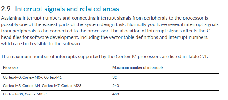
2.9 Interrupt Signals and Related Areas
Assigning interrupt numbers and connecting interrupt signals from peripherals to the processor is possibly one of the easiest parts of the system design task.
-> 인터럽트 번호를 부여하고 Peripherals 의 신호를 프로세서에 연결
Normally you have several interrupt signals from peripherals to be connected to the processor. The allocation of interrupt signals affets the C head files for softare devlopment, including the vector table definitions and interrupt numbers, which are both visible to the software.
-> 인터럽트 할당은 C header 에서 보통 한다.
If the number of interrupt signals exceeds the maximum number support, it is possible to merge multiple interrupt lines and share one interrupt service routine(ISR) and determine which interrupt to be serviced in the ISR by software
-> interrupt 숫자가 부족하면 여러 신호를 하나의 interrupt service routinge 에 엮을 수 있다.
On all currnet Cortex-M processors, the interrupt signals:
Are active high and must be synchronous to the processor's system clock;
Can be level triggered or pulse triggered. if using pulse triggered, the duration of the pulse must be at least one clock cycle.
-> Pulse trigger 된다. 하나의 클락의 duration 이 필요.
The unused of not implemented interrupt input pins should be tied to 0 and must not be allowed to enther unknown state 'X'. (e.g., if a peripheral outputs X in its interrupt line when the peripheral is powered down, the signal level must be clamped to 0 before the power down happened). Issues with unknown or 'X' signal values generally affect simulation but represent possible unexpercted values when using ASIC or FPGA
-> 인터럽트는 쓰지 않을 경우 0 으로 tied 되어야 한다.
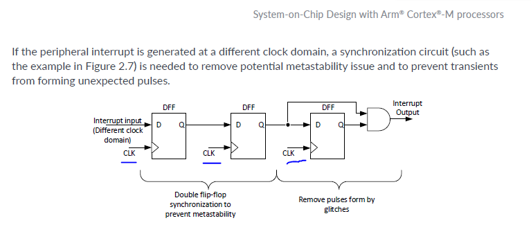
if the peripheral interrupt is generated at a diferent clock domain, a synchronization circuit ( such as the example in Figrue 2.7 ) is needed to remove potential metastabuility issue and to prenent transients from forming unexpected pulses.
-> CDC interrupt
Cortex-M processors have an Non-Maskable Interrupt(NMI) Input. In common embedded systems the NMI could be connected to:
- Voltage monitoring logic (also known as brownout detector) to ensure that the system is shut down correctly when support voltage drops to a certain value or
- The NMI could be connected to a watchdog time to carry out remedial actions if the system has stopped normal operation.
-> NMI 는 보통 Watchodg error interrupt 나 voltage monitoring error 일때 쓴다.
NMI is unlikely to be used as the interrupt for normal peripherals.
This is because the built-in interrupt controller NVIC already provides interrupt prioritization, so each peripheral can already be programmed as ther highest priority by just using the normal IRQ conncetion. Also, a fault generated within the NMI handler ca cause the processor to enter lockup state, which ca nbe problematic for some applications. Faults in normal interrupt handlers allow the Hard Fault handler (or other configuraable fault handlers) to be triggered and excuted.
-> NVIC는 내부적으로 이미 Interrupt가 우선순위가 높게 되 있음. 그렇기 때문에 일반 peripheral 은 이미 normal IRQ connection 으로 연결 되있고 , 또한 NMI 로 발생된 Interrupt 는 processor 도 lockup state에 들게 할 수 있음.
Another characterisic of the NVIC is that it can handle interrupt requests om the form of pulse as well as level signal. if a peripheral generates an interrupt request in the form of a pulse signal, the request is held by pending status within the NVIC until the interrupt reqeust in ther form of a level signal, the interrupt handler must clear the request at the peripheral.

level signal 로 interrupt 가 발생했으면 핸들러는 periheral 요청을 clear 해줘야함.
펄스 신호 인터럽트 요청을 처리하기 위해서는, NVIC는 보통 우선순위를 결정하고 CPU가 처리할 수 있도록 큐에 요청을 추가합니다. CPU가 인터럽트를 처리할 준비가 되면, NVIC는 인터럽트 핸들러 코드로 적절한 인터럽트 벡터를 보내고, 이를 통해 인터럽트를 처리합니다.
인터럽트도 큐가 있다.
The key advantage of a pulsed interrupt is theat it save a few clock cycles in the ISR that there is no need to clear the interrupt requests at the peripherals. However, in many cases, a level-triggered interrupt is preferred because :
- Cross clock domain synchronization of level-triggered interrupts is simpler than pulsed interrupts.
in ther case where pulse interrupt synchronization logic is used, two successive interrupt request pulses could be merged into one after the syronizer due to the latency of the synchornization,which can be confusing.
-> 두개의 연속된 인터럽트가 있으면 합쳐 질수도 있다.
