System-on-Chip Design with Arm® Cortex®-M processors -12
For FPGA designs, instead of using the behavioral model for ROM and RAM, the memory will be relaced by either :
-
Memory blocks within the FPGA device, or
-
External memory devices
-
In cases where the memories are to be implemented inside the FPGA, the design flow can involve:
-
Using the memory generator in your FPGA development tool to generate the required memory block design file, or
-
Instantiating the required memory component directly in the FPGA design library.
If the synthesis tool supports the synthesis of memory models, we can create a synthesizable memory model and synthesize the design together with other Verilog files.
In all casesm the implementation details depend on the FPGA product that you are using as well as the devleopment tools.
For example, for users of Synplify, they can choose to synthesize a behavior model of memory, with the possibility of using a standar Verilog function like "$readmemh" to specify the initial content of the memory. The tools will then create the memory blocks in the FPGA. A similar fearture is also availble
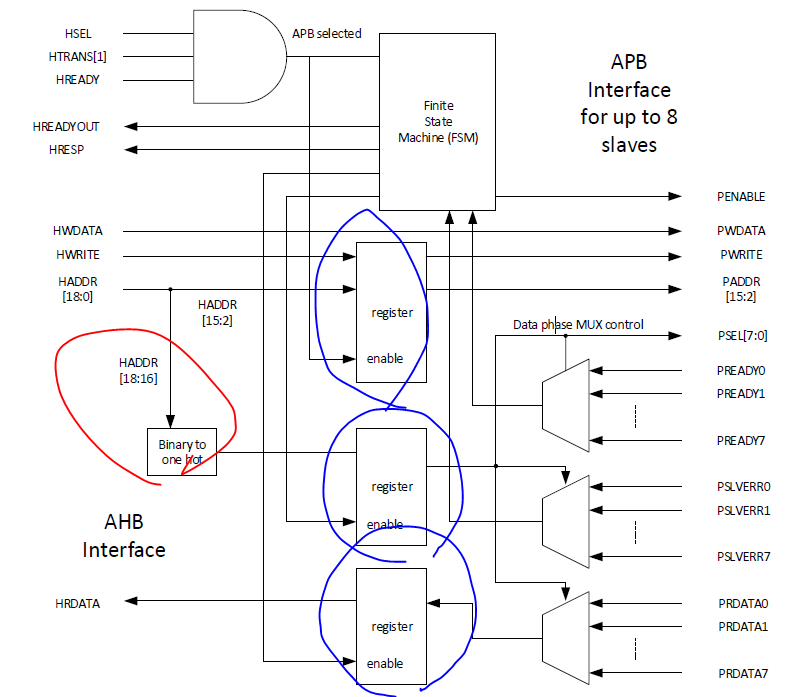
7.3.5 AHB to APB Bridge
The AHB to APB Brdige is needed when connecting peripherals with an APB interface to an Arm processor that has an AHB interface.
the unused input signals on the bridge such as PREADY input signal can be tied to 1, and the PSLVERR input signal can be tied low.
In AHB, the address value and control information are output from the bus masater during the address phase.
Since the duration of the address pahse is no fixed and the write data is not available undil data phse, the bus bridge registers the address and read/write control signal at the end of the address phase and outputs thme to the APB during the data pahse.
In order to generate the requiresed PSEL and PENABLE signals, the bus bridge contains a simple FSM to handel the APB control signals, as well as generating an error reponse o n the AHB when an APB slave error(PSLVERR) is asserted.
The example design also includes an APB slave mlutiplexer and eight interface ports to APB slaves. The selection of which slave to access is determined by bit-14 to bit 12 of the address value(HADDR[14:12]). It is possible to design the APB Bridege and the APB slave multiplexer as two spearated units. However, in this example, they have been designed as a single unit to simplify integration of the AMBA system.
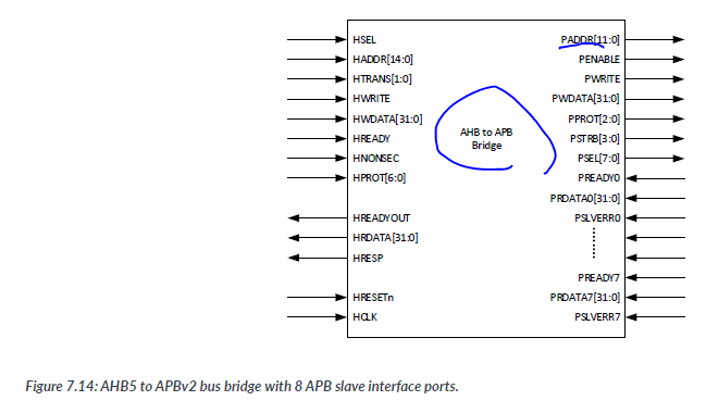
The example bus bridge design assumes that HCLK is the same as PCLK. If the AHB system and APB system have different clock frequencies, ir if the clock signals are asynchronous, the bus bridge will have to include an extra handshaking mechanism to support the data transfers across different clock domains, This is not supported on the example bridge iscussed here.
To keep the design simple, we habe also omitted exclusive access support, as semaphore data are normally placed in SRAM rather than in peripherals.
For a simple read operation the bridge ouputs the address and APB control signal at the beginning of the data phase.
When the read data is obtained, the read value is sampled in a register and output to the AHB system in the next clock cycle. Since the bridge supports multipl APB slave interfaces, there are multiple PSEL, PRDATA, PSLVERR, and PREADY signals,which have a number as their suffix.
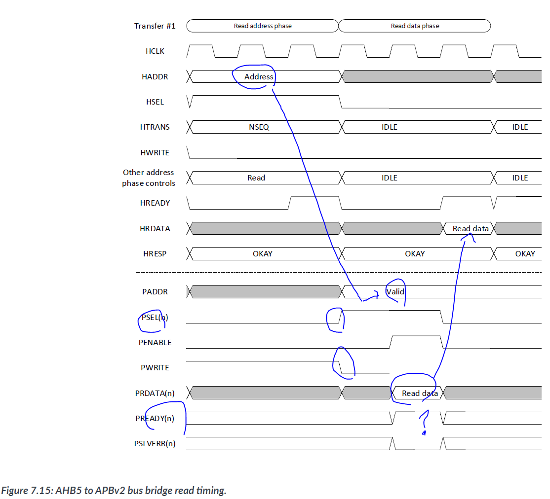
It is possible to design the bridge so that as soon as the read data is ready, it is passed on to the AHB system without the samlping cycle. However, this could result in poor timing performance if the output delay of the peripheral system is high, or if the processor core requires a longer setup time for the read data. Registering the read data signal and read response provides better synthesis timing performance for the ASIC/FPGA design. The disadvantage is that it slightly increases the area of the design and adds an extran clock cycle for APB operations.
읽은 데이터가 준비되는 즉시 AHB 시스템으로 전달되도록 브릿지를 설계하는 것은 가능합니다. 그러나 이 경우 주변장치 시스템의 출력 지연이 크거나 프로세서 코어가 읽은 데이터에 대해 더 긴 설정 시간을 요구하는 경우에는 타이밍 성능이 저하될 수 있습니다. 읽은 데이터 신호와 읽은 응답을 레지스터에 등록하는 것은 ASIC/FPGA 설계의 합성 타이밍 성능을 더욱 향상시킵니다. 이러한 방식의 단점은 설계의 면적을 약간 증가시키고 APB 동작에 추가적인 클록 사이클을 추가한다는 것입니다.The write transfer bridging is similart to read transfer. For write data, in most cases, it is not a problem to connect from HWDATA directly to PWDATA becuase there is no need to add a multiplexer in the write data path(only buffers are needed as the HWDATA signals are connected to large number of bus slaves). But the PREADY and PSLVERR signals are registered before feeding back to AHB system.
In orger to generate the read and wrtie control signals, a simple FSM is used.
The FSM is also used to generate the two-cycle error reponse on the AHB if an error response on the APB is detected.
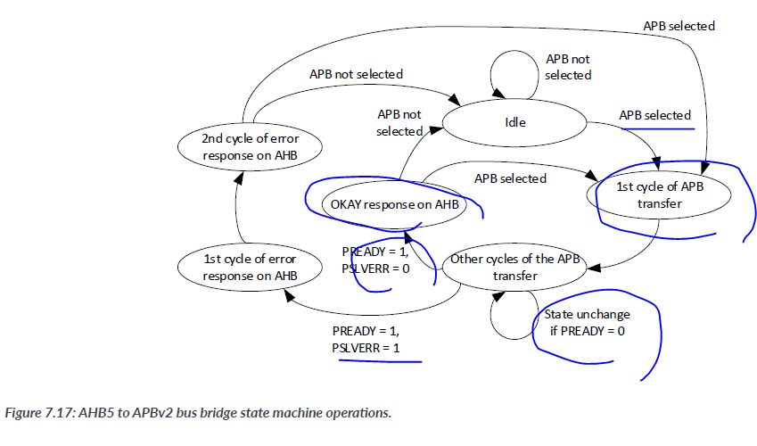
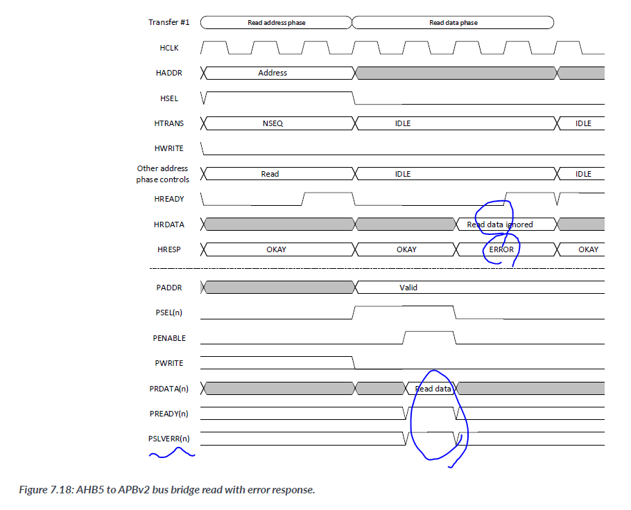
If a slave error is detected on the APB bus, the APB bridge needs to generate an error response to the AHB master. The error reponse on the AHB muster be two cycles in lenght. Therefore, two states are assigned in the FSM for this pupose. For example, if an APB receives an error from the peropheral(PSLVERR - 1), the wave form would look like :
The same applies to the bridging write transfers. if an APB write transfer receives an error reponse, the bus bridge generates the error response using the same mechanism.
Based on these waveforms, we could design the AHB to APB Bridge, as shown in the following block diagram :
-
HSEL , HTRANS[1], HREADY 를 가지고 FSM 이
-
PENABLE 신호를 정한다. 또한 Register 를 Enable 한다.
-
Register은 PWRITE PADDR 를 받아서 전달하고
-
HADDR 의 18:16 bit 의 정보를 가지고 PREADY, PSLVERR, PRDATA 의 어떤 데이터를 받을 지를 결정한다. -> The selection of which slave to access is determined by bit-14 to bit 12 of the address value(HADDR[14:12]).
up to eight APB slave can be connected to the bridge. 14:12
This can be done by changing the binary to ont-hot logic, the PSEL register, and the multiplexer.
The current design allows each APB to take up 4kB of memory. If the memory range for each APB slave needs to be increase or decreased, the address signal lines connected to the slave multiplexer need to be changed. In most cases, 4KB should be enough for msot imple APB slaves.
7.4 Bridging from Cortex-M3/Cortex-M4 AHB Lite to AHB5
A simple bus wrapper component is needed to brdige the AHB interface
-Conversion of memory attribute sideband signals to new AHB5 HPROT signals ;
- Conversion of exclusive access signals.
HRESP input signals on hte Cortex-M3 processor are 2-bit wide as they are in AHB, although the RETRY and SPILT responses are not supported. When connecting a Cortex-M3 processor to AHB Lite infrastructure, the bit 1 of the HRESP input in the processor can be tied to 0. Since Cortex-M4 was designed to enable easy migration from Cortex-M3, it kept the same arrangement, and therefore its HRESP inputs are also 2-bit wide.
In this bus wrapper, we omitted the HNONSEC(Security Attrubute for TrustZone Support). If a Cortex-M processor without TrustZuone support is used in a TrustZone enabled system, you can use on of two arangement.
-
The Cortex-M processor is treated as always Non-secure. In this case, the HONSEC signal(s) of the Cortex-M procesoor is tied high. The bus system needs to handle permission checking to prevent the processor from accessing Secure memories.
-
The Cortex-M processor is treated as always Secure. In this case, the HNONSEC signal must be generated based on the memory address partiioning.
The Corstone system design kis from Arm provide a component called Master Security Controller to handle security management of legacy bus masters in a TrustZone based system.
