Design of simple peripherals
if you are designing a peripheral for a Cortex-M processor-based system or setting out to develop wrapper for legacy 8-bit or 16-bit peropheral blocks, a number of standard practives will make the software development easier :
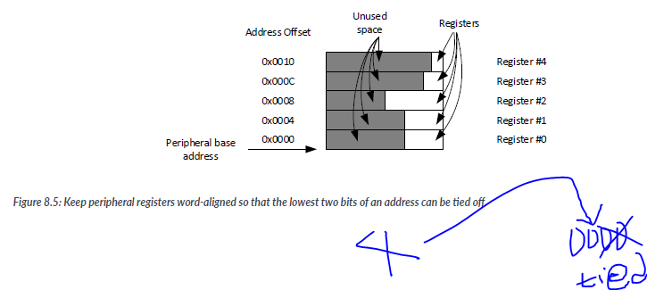
- Make sue that the peripheral;s registers are word-aligned unless you ar creating an AHB pripheral with byte0addressable registers. In most cases, peripherals will be connected to the APB bus system. Since there is no transfer size information on this bus and the bus size is always 32-bit wide, it is best to make every register word size and align to word addresses. At the peripheral interface, the address bit [1:0] is unused and can be ignored.
워드 정렬(word-aligned)이란 레지스터가 워드 크기(32비트 또는 4바이트)의 배수 주소에서 시작함을 의미합니다. 이렇게 하면 버스에서 레지스터에 효율적으로 액세스할 수 있습니다. 레지스터를 워드 주소에 정렬하면 바이트 단위 액세스를 사용하지 않거나 비정렬 액세스를 처리할 필요가 없어지므로 설계가 단순화되고 성능 부하가 줄어듭니다.- When creating peripheral registers, it is important to avoid a status bit that can be cleared by writing a zero to it. For example, if the application needs to perform a read-modify-write operation to change a one-bit bitfield value in a peripheral register, and if another status bit of the same register changed state between the read and the write access, the information of the status bit change would be lost when the write-back taks place. Normall, status bits that indicate events can be implemted as write 1 to celar. In this way, the status bit will not be leared accidetally.
-> ???
쓰기백 작업이 발생하면, 주변장치의 변경된 데이터가 메모리로 전송되고 주변장치의 캐시나 레지스터에 저장됩니다. 이렇게 함으로써 다른 주변장치나 프로세서가 해당 데이터를 읽을 때, 최신의 데이터를 제공할 수 있습니다.- When creating status registers in peripherals, it is best to avoid a status register that changes its value upon read accesses(e.g., clear on read). This is becuase you might want to read the peripheral memroy map through a debugger at teh time as the program is running. Of course sometimes, this cannot be avoided. In this cases, you might want to create a separate address for the debugger accesses to the peripheral status register so that reading of status information by the debugger will not change the behavior of the devide.
-> 주변장치의 상태 레지스터를 생성할 때, 읽기 액세스에 따라 값이 변경되는 상태 레지스터(예: 읽을 때 초기화)를 피하는 것이 가장 좋습니다.
Be aware that the status of the peripheral interface might be in an undefined state during the starting up of an FPGA. internally to the FPGA, the peripheral can be reset after the FPGA is ready. But the external circuit interface to the peripheral will need to be aware that the FPGA needs a certain period of time to get ready. Most FPGA products have status output to indicate that the starting sequence is completed. This can be used to externally disable the circuit from activation.
FPGA의 시작 시에는 초기화 및 구동 프로세스가 진행되는 동안 주변장치 인터페이스의 상태가 정의되지 않은 상태일 수 있습니다. 이는 FPGA가 전원이 인가되고 구동되는 동안 초기화, 구성 및 다른 내부 동작을 수행하는 과정에서 발생할 수 있는 일입니다.

FPGA가 시작되고 주변장치가 초기화되는 동안에는 외부 회로 인터페이스는 이러한 상태의 불확실성을 고려해야 합니다. FPGA가 완전히 시작되고 준비되기까지 일정 시간이 소요될 수 있으므로 이에 대한 대기 기간을 고려해야 합니다.- In most caes, interrupt signals from peripherals are designed as level trigger interrupts. Compared to pulse triggered interrupts, level trigger interrupts can propagate through clock domains with simple synchronizers. Whereas synchroniation for pulse trigger interrupt signals is more complex.
When developing a complex design, it is often impractical to design all of the required peripherals by yourself. However, there are vaiouf offerins available from intellectaul Propeory providers that can be used to create peripheral soulitions that work with Arm processors. Arm also has arange of peripheral products and subsystem products for accelerating time to market.
In many cases, a peripheral could operate at a much slower clock speed than the processor. Instead of using bus bridges to convert the bus clock speed to match the peripheral speed, it is often best to have a separated clock for the bus interface of the peripheral and a clock fro peripheral functions. The complexity of the peripheral would increase as as result, as there is need for addition synchronization logic between the clock domains. However, this arrangement avoids high access latency when reading/writing to the peripheral registers, which reduces the energy efficiency of the system and has an impact on interrupt latncy.
많은 경우, 주변 장치는 프로세서보다 훨씬 느린 클럭 속도에서 동작할 수 있습니다. 버스 브릿지를 사용하여 버스 클럭 속도를 주변 장치 속도에 맞추는 대신, 주변 장치의 버스 인터페이스를 위한 별도의 클럭과 주변 장치 기능을 위한 클럭을 사용하는 것이 가장 좋을 때가 많습니다. 이러한 경우에는 클럭 도메인 간에 추가적인 동기화 논리가 필요하기 때문에 주변 장치의 복잡성이 증가합니다. 그러나 이러한 구성은 주변 레지스터 읽기/쓰기 시에 높은 액세스 대기 시간을 피할 수 있으며, 이로 인해 시스템의 에너지 효율성이 감소하고 인터럽트 지연에 영향을 줄 수 있습니다.8.2 Designing Simple APB Peripherals
For the majority of peripheral designs, the AMBA APB protocol is usually chosen because it is very simple. There are, of course, situations where peripherals need to be designed with an AHB interface instead. For example, if a peripheral is required to support any of the following :
-
Transfers of different data sizeS(registers are byte/half-word addressable),
-
Exclusive accesses, or
-
Instances in which the peripheral needs to behave differently when other bus-masters have access to it.
대부분의 주변 장치 설계에서는 매우 간단한 AMBA APB 프로토콜이 일반적으로 선택됩니다. 물론 주변 장치를 AHB 인터페이스로 설계해야 하는 상황도 있습니다. 예를 들어, 주변 장치가 다음 중 하나를 지원해야 하는 경우입니다:

다른 데이터 크기의 전송 (레지스터가 바이트/하프워드 단위로 접근 가능한 경우)
독점 액세스
다른 버스 마스터가 액세스할 때 주변 장치가 다르게 동작해야 하는 경우 (참고: HMASTER 신호가 필요함)
In this section, we will cover the design of simple APB peripherals, including a simple parallel I/O interfae and a simple timer. First of all, though, we will take a look at APB interface desgin in general.
APB transfer take two cycles in AMBA 2, or a minimum of two ccles in AMBA3 and later version.
For read operations, an APB salve must procide valid read data at the last cycle of the transfer, except when it is responding with an error signal(applicable only in AMBA 3). For slower frequency systems, we can generate the read data as soon as possible without any pipeline stage.
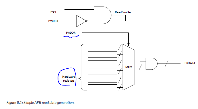
With the arrangement shown in Figure 8.1, the PRDATA will be valid for all the cycles during the APB transfer. however, in systems that require higher operating frequency , this design migh not be suitable because of the propagation delay in the read data generation.
For example, if an APB slave contains a large number of hardware registers, the rad data multiplexer will have a long delay.In addition to that, the APB slave multiplexer at the system level(in our example the APB slave multiplexer is built in to the AHB to APB) also requires some time to multiplex the read data from different APB slaves.
As a result, the total propagation delay can be quite significant and can be worse when we include wire connection delays in the calculation. This can reduce the maximum clock frequency of the system, or caouse signal routing problems within the FPGA/ASIC designs.
In order to solve this problem, we can insert a register stage in the APB slave read data interface to improve the synthesis timing of the data path. The pipeline stage could be inserted in different positions, depending on your design. One of the possible arragements is to register the read data mlutiplexer output.
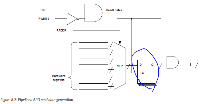
By using this pipeline stage, we can prevent the signal path from hardware registers within the APB slaves to the AHB to APB bridge, so in total, a data read takes two clock cycles to get the data value from the peripheral register to the processor. This seems to have increased the read operation latency, but the first registering cycle within the APB slave overlapped with the APB operations(APB transfers take a minimum of two cycles), so the only extra latency cycle is at the registering stage fof the AHB to APB bridge.
->
이렇게 함으로써 데이터 읽기 작업의 지연 시간이 증가하였지만, APB 슬레이브 내의 레지스터링과 APB 동작이 겹쳐짐으로써 추가적인 클록 사이클을 최소화할 수 있습니다. 따라서 전체적인 지연은 AHB에서 APB로의 브릿지의 레지스터링 단계에서 발생하는 하나의 클록 사이클만 추가됩니다.

In the example designs , the register slices for read data only activate if there is a read to the slave. Otherwise, the register is held unchanged to reduce power consumption. The read data output (PRDATA) is masked by a ReadEnable signal to block data output when the APB slave is not being read.
-> 이러한 설계 방식은 읽기 동작이 발생하지 않을 때 데이터 출력을 차단하여 전력 소비를 줄이는데 도움이 됩니다.
Such a blocking mechanism could potentailly simplify merging of PRDATA from multiple slaves by using just OR logic if all bus slaves in the APB segment has the same behavior.
The write operation is easier to implement. For example, if each writeable hardware register has a corresponding write enable signals, the write enable signal can be generated as :
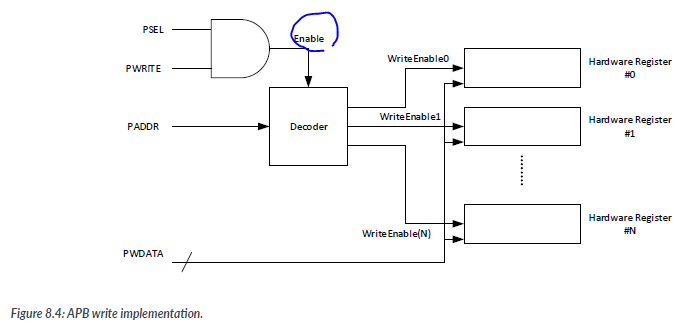
When designing APB peripherals, we should assign each hardware register to word-aligned addresses and reserve the whole word for the register even if only part of the space is used. This is because the APB interface does not provide transfer size information, so each access is assumed to be the maximum transfer size of the bus(i.e., word size). The common practive is that bit 1 and bit 0 of the PADDR bus are not used, and register are assigned with word aligned addresses like (0xXXXX000, 0xXXXX0004). Even if the register does not require does not require the whole word, it occupies the whole word address.
-> APB 주변 장치를 설계할 때, 각 하드웨어 레지스터를 워드에 맞춘 주소에 할당하고, 공간의 일부만 사용되는 경우에도 전체 워드를 레지스터에 예약해야 합니다. 이는 APB 인터페이스가 전송 크기 정보를 제공하지 않기 때문에, 각 액세스는 버스의 최대 전송 크기(즉, 워드 크기)로 가정되기 때문입니다.
In most cases, these peripherals have three peripherals have three read and write control signals : Chip-Select, Read-Enable, and Write-Enable. If the peripheral has a synchronous(clocked) interface and does not require a tristate dat bus, it is normally an easy task to connect this type of peripheral to APB.
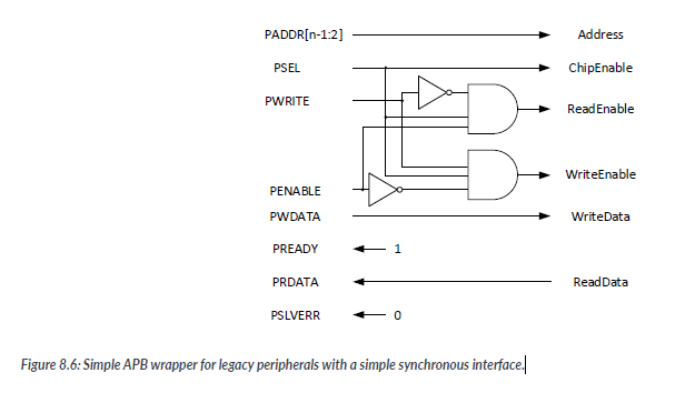
However, if the peripheral requires tristate bus interface, or uses an asynchronous interface, the wrapper will have to handle the transfer in multiple clock cycles and create a trun-around cycle if a tristate bus is used( a turn - around cycle is used to prevent current spikes on the data bus when the direction of the data changes,
