<최근 업데이트(24.08.04)>
별거없는데 DAC에 맞는 clock을 만들어준 부분을 추가했다.
16384(DAC가 14비트임->2의 14승개 데이터)개의 data를 400us 안에 처리한다고 생각하면(실제로는 200us안에 처리해야함->클럭 2배로 만들면 되는데 귀찮으니까 나중에 함)
1초에는 40,960,000 data를 처리해야 함(40MSPS) 3배 했을 때 165MSPS 안에 들어온다.
그러면 1개의 data를 처리할 때 24ns 정도 걸리게 됨. -> LSB의 한 주기가 24ns 걸려야 한다는 뜻
xdc(constraint) 파일에서도 원하는 주파수 가진 클럭 만들 수 있는데 잘 안돼서 clocking wizard 방법으로 클럭 생성함
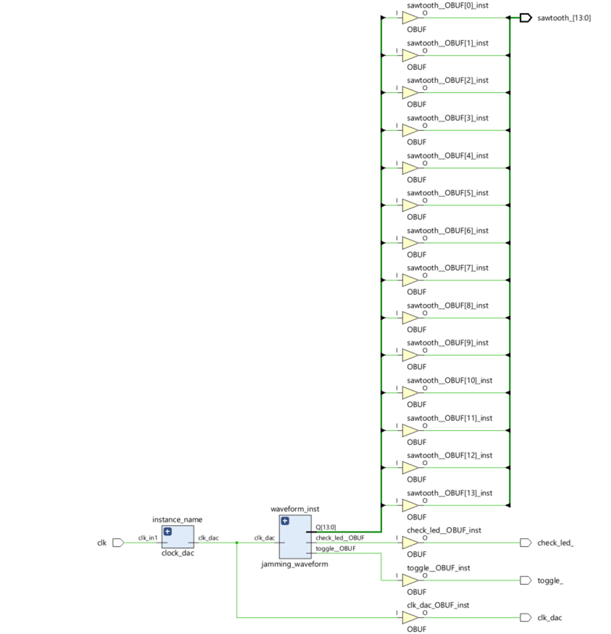
//top모듈(클럭 생성+파형 생성)
`timescale 1ns / 1ps

module top(
input clk, output clk_dac,  output  [13:0] sawtooth_, output check_led_, output  toggle_
    );

      clock_dac instance_name
   (
    // Clock out ports
    .clk_dac(clk_dac),     // output clk_dac //들어온 clk_in1으로 clk_dac만들고 output으로 내보냄
    // Clock in ports
    .clk_in1(clk)      // input clk_in1 //입력받는 신호 clk을 clk_in1에 넣어서
    //근데 clocking wizard에서 clk_in1에 시스템 클럭(125MHz)할당해놓음.
);

  jamming_waveform waveform_inst (
    .clk(clk_dac),  // Clocking Wizard에서 생성된 클럭 신호(clk_dac) 사용
    .sawtooth(sawtooth_),
    .check_led(check_led_),
    .toggle(toggle_)
  );

endmodule
//이전 포스트에 올렸던 파형 생성 소스코드와 동일
`timescale 1ns/1ps
module jamming_waveform(input clk, output reg [13:0] sawtooth, output reg check_led, output reg toggle);
//reg [31:0] real_count=0; //1초 count 위해서


localparam sawtoothPeriod=16384;

initial begin sawtooth=14'b0; check_led=1'b0; toggle=1'b0; end
always@(posedge clk)
begin
if(sawtooth==(sawtoothPeriod-1)) sawtooth <=0;
else begin
sawtooth <= sawtooth+1'b1; check_led=~check_led; toggle=~toggle; end
end

endmodule
//constraint(FPGA의 어떤 핀에 어떤 신호 할당하겠다고 정의해주는 파일)-샵 없는 line(핀)들이 활성화해서 사용하겠다
## This file is a general .xdc for the Zybo Z7 Rev. B
## It is compatible with the Zybo Z7-20 and Zybo Z7-10
## To use it in a project:
## - uncomment the lines corresponding to used pins
## - rename the used ports (in each line, after get_ports) according to the top level signal names in the project
##Clock signal
set_property -dict { PACKAGE_PIN K17 IOSTANDARD LVCMOS33 } [get_ports { clk }]; #IO_L12P_T1_MRCC_35 Sch=sysclk
#create_clock -add -name sys_clk_pin -period 24.00 -waveform {0 12} [get_ports { clk_in1 }];
##Switches
#set_property -dict { PACKAGE_PIN G15 IOSTANDARD LVCMOS33 } [get_ports { sw[0] }]; #IO_L19N_T3_VREF_35 Sch=sw[0]
#set_property -dict { PACKAGE_PIN P15 IOSTANDARD LVCMOS33 } [get_ports { sw[1] }]; #IO_L24P_T3_34 Sch=sw[1]
#set_property -dict { PACKAGE_PIN W13 IOSTANDARD LVCMOS33 } [get_ports { sw[2] }]; #IO_L4N_T0_34 Sch=sw[2]
#set_property -dict { PACKAGE_PIN T16 IOSTANDARD LVCMOS33 } [get_ports { sw[3] }]; #IO_L9P_T1_DQS_34 Sch=sw[3]
##Buttons
#set_property -dict { PACKAGE_PIN K18 IOSTANDARD LVCMOS33 } [get_ports { btn[0] }]; #IO_L12N_T1_MRCC_35 Sch=btn[0]
#set_property -dict { PACKAGE_PIN P16 IOSTANDARD LVCMOS33 } [get_ports { btn[1] }]; #IO_L24N_T3_34 Sch=btn[1]
#set_property -dict { PACKAGE_PIN K19 IOSTANDARD LVCMOS33 } [get_ports { btn[2] }]; #IO_L10P_T1_AD11P_35 Sch=btn[2]
#set_property -dict { PACKAGE_PIN Y16 IOSTANDARD LVCMOS33 } [get_ports { btn[3] }]; #IO_L7P_T1_34 Sch=btn[3]
##LEDs
#set_property -dict { PACKAGE_PIN M14 IOSTANDARD LVCMOS33 } [get_ports { led[0] }]; #IO_L23P_T3_35 Sch=led[0]
#set_property -dict { PACKAGE_PIN M15 IOSTANDARD LVCMOS33 } [get_ports { led[1] }]; #IO_L23N_T3_35 Sch=led[1]
#set_property -dict { PACKAGE_PIN G14 IOSTANDARD LVCMOS33 } [get_ports { led[2] }]; #IO_0_35 Sch=led[2]
#set_property -dict { PACKAGE_PIN D18 IOSTANDARD LVCMOS33 } [get_ports { led[3] }]; #IO_L3N_T0_DQS_AD1N_35 Sch=led[3]
##RGB LED 5 (Zybo Z7-20 only)
set_property -dict { PACKAGE_PIN Y11 IOSTANDARD LVCMOS33 } [get_ports { check_led_ }]; #IO_L18N_T2_13 Sch=led5_r
#set_property -dict { PACKAGE_PIN T5 IOSTANDARD LVCMOS33 } [get_ports { led5_g }]; #IO_L19P_T3_13 Sch=led5_g
#set_property -dict { PACKAGE_PIN Y12 IOSTANDARD LVCMOS33 } [get_ports { led5_b }]; #IO_L20P_T3_13 Sch=led5_b
##RGB LED 6
#set_property -dict { PACKAGE_PIN V16 IOSTANDARD LVCMOS33 } [get_ports { led6_r }]; #IO_L18P_T2_34 Sch=led6_r
#set_property -dict { PACKAGE_PIN F17 IOSTANDARD LVCMOS33 } [get_ports { led6_g }]; #IO_L6N_T0_VREF_35 Sch=led6_g
#set_property -dict { PACKAGE_PIN M17 IOSTANDARD LVCMOS33 } [get_ports { led6_b }]; #IO_L8P_T1_AD10P_35 Sch=led6_b
##Audio Codec
#set_property -dict { PACKAGE_PIN R19 IOSTANDARD LVCMOS33 } [get_ports { ac_bclk }]; #IO_0_34 Sch=ac_bclk
#set_property -dict { PACKAGE_PIN R17 IOSTANDARD LVCMOS33 } [get_ports { ac_mclk }]; #IO_L19N_T3_VREF_34 Sch=ac_mclk
#set_property -dict { PACKAGE_PIN P18 IOSTANDARD LVCMOS33 } [get_ports { ac_muten }]; #IO_L23N_T3_34 Sch=ac_muten
#set_property -dict { PACKAGE_PIN R18 IOSTANDARD LVCMOS33 } [get_ports { ac_pbdat }]; #IO_L20N_T3_34 Sch=ac_pbdat
#set_property -dict { PACKAGE_PIN T19 IOSTANDARD LVCMOS33 } [get_ports { ac_pblrc }]; #IO_25_34 Sch=ac_pblrc
#set_property -dict { PACKAGE_PIN R16 IOSTANDARD LVCMOS33 } [get_ports { ac_recdat }]; #IO_L19P_T3_34 Sch=ac_recdat
#set_property -dict { PACKAGE_PIN Y18 IOSTANDARD LVCMOS33 } [get_ports { ac_reclrc }]; #IO_L17P_T2_34 Sch=ac_reclrc
#set_property -dict { PACKAGE_PIN N18 IOSTANDARD LVCMOS33 } [get_ports { ac_scl }]; #IO_L13P_T2_MRCC_34 Sch=ac_scl
#set_property -dict { PACKAGE_PIN N17 IOSTANDARD LVCMOS33 } [get_ports { ac_sda }]; #IO_L23P_T3_34 Sch=ac_sda
##Additional Ethernet signals
#set_property -dict { PACKAGE_PIN F16 IOSTANDARD LVCMOS33 PULLUP true } [get_ports { eth_int_pu_b }]; #IO_L6P_T0_35 Sch=eth_int_pu_b
#set_property -dict { PACKAGE_PIN E17 IOSTANDARD LVCMOS33 } [get_ports { eth_rst_b }]; #IO_L3P_T0_DQS_AD1P_35 Sch=eth_rst_b
##USB-OTG over-current detect pin
#set_property -dict { PACKAGE_PIN U13 IOSTANDARD LVCMOS33 } [get_ports { otg_oc }]; #IO_L3P_T0_DQS_PUDC_B_34 Sch=otg_oc
##Fan (Zybo Z7-20 only)
#set_property -dict { PACKAGE_PIN Y13 IOSTANDARD LVCMOS33 PULLUP true } [get_ports { fan_fb_pu }]; #IO_L20N_T3_13 Sch=fan_fb_pu
##HDMI RX
#set_property -dict { PACKAGE_PIN W19 IOSTANDARD LVCMOS33 } [get_ports { hdmi_rx_hpd }]; #IO_L22N_T3_34 Sch=hdmi_rx_hpd
#set_property -dict { PACKAGE_PIN W18 IOSTANDARD LVCMOS33 } [get_ports { hdmi_rx_scl }]; #IO_L22P_T3_34 Sch=hdmi_rx_scl
#set_property -dict { PACKAGE_PIN Y19 IOSTANDARD LVCMOS33 } [get_ports { hdmi_rx_sda }]; #IO_L17N_T2_34 Sch=hdmi_rx_sda
#set_property -dict { PACKAGE_PIN U19 IOSTANDARD TMDS_33 } [get_ports { hdmi_rx_clk_n }]; #IO_L12N_T1_MRCC_34 Sch=hdmi_rx_clk_n
#set_property -dict { PACKAGE_PIN U18 IOSTANDARD TMDS_33 } [get_ports { hdmi_rx_clk_p }]; #IO_L12P_T1_MRCC_34 Sch=hdmi_rx_clk_p
#set_property -dict { PACKAGE_PIN W20 IOSTANDARD TMDS_33 } [get_ports { hdmi_rx_n[0] }]; #IO_L16N_T2_34 Sch=hdmi_rx_n[0]
#set_property -dict { PACKAGE_PIN V20 IOSTANDARD TMDS_33 } [get_ports { hdmi_rx_p[0] }]; #IO_L16P_T2_34 Sch=hdmi_rx_p[0]
#set_property -dict { PACKAGE_PIN U20 IOSTANDARD TMDS_33 } [get_ports { hdmi_rx_n[1] }]; #IO_L15N_T2_DQS_34 Sch=hdmi_rx_n[1]
#set_property -dict { PACKAGE_PIN T20 IOSTANDARD TMDS_33 } [get_ports { hdmi_rx_p[1] }]; #IO_L15P_T2_DQS_34 Sch=hdmi_rx_p[1]
#set_property -dict { PACKAGE_PIN P20 IOSTANDARD TMDS_33 } [get_ports { hdmi_rx_n[2] }]; #IO_L14N_T2_SRCC_34 Sch=hdmi_rx_n[2]
#set_property -dict { PACKAGE_PIN N20 IOSTANDARD TMDS_33 } [get_ports { hdmi_rx_p[2] }]; #IO_L14P_T2_SRCC_34 Sch=hdmi_rx_p[2]
##HDMI RX CEC (Zybo Z7-20 only)
#set_property -dict { PACKAGE_PIN Y8 IOSTANDARD LVCMOS33 } [get_ports { hdmi_rx_cec }]; #IO_L14N_T2_SRCC_13 Sch=hdmi_rx_cec
##HDMI TX
#set_property -dict { PACKAGE_PIN E18 IOSTANDARD LVCMOS33 } [get_ports { hdmi_tx_hpd }]; #IO_L5P_T0_AD9P_35 Sch=hdmi_tx_hpd
#set_property -dict { PACKAGE_PIN G17 IOSTANDARD LVCMOS33 } [get_ports { hdmi_tx_scl }]; #IO_L16P_T2_35 Sch=hdmi_tx_scl
#set_property -dict { PACKAGE_PIN G18 IOSTANDARD LVCMOS33 } [get_ports { hdmi_tx_sda }]; #IO_L16N_T2_35 Sch=hdmi_tx_sda
#set_property -dict { PACKAGE_PIN H17 IOSTANDARD TMDS_33 } [get_ports { hdmi_tx_clk_n }]; #IO_L13N_T2_MRCC_35 Sch=hdmi_tx_clk_n
#set_property -dict { PACKAGE_PIN H16 IOSTANDARD TMDS_33 } [get_ports { hdmi_tx_clk_p }]; #IO_L13P_T2_MRCC_35 Sch=hdmi_tx_clk_p
#set_property -dict { PACKAGE_PIN D20 IOSTANDARD TMDS_33 } [get_ports { hdmi_tx_n[0] }]; #IO_L4N_T0_35 Sch=hdmi_tx_n[0]
#set_property -dict { PACKAGE_PIN D19 IOSTANDARD TMDS_33 } [get_ports { hdmi_tx_p[0] }]; #IO_L4P_T0_35 Sch=hdmi_tx_p[0]
#set_property -dict { PACKAGE_PIN B20 IOSTANDARD TMDS_33 } [get_ports { hdmi_tx_n[1] }]; #IO_L1N_T0_AD0N_35 Sch=hdmi_tx_n[1]
#set_property -dict { PACKAGE_PIN C20 IOSTANDARD TMDS_33 } [get_ports { hdmi_tx_p[1] }]; #IO_L1P_T0_AD0P_35 Sch=hdmi_tx_p[1]
#set_property -dict { PACKAGE_PIN A20 IOSTANDARD TMDS_33 } [get_ports { hdmi_tx_n[2] }]; #IO_L2N_T0_AD8N_35 Sch=hdmi_tx_n[2]
#set_property -dict { PACKAGE_PIN B19 IOSTANDARD TMDS_33 } [get_ports { hdmi_tx_p[2] }]; #IO_L2P_T0_AD8P_35 Sch=hdmi_tx_p[2]
##HDMI TX CEC
#set_property -dict { PACKAGE_PIN E19 IOSTANDARD LVCMOS33 } [get_ports { hdmi_tx_cec }]; #IO_L5N_T0_AD9N_35 Sch=hdmi_tx_cec
##Pmod Header JA (XADC)
#set_property -dict { PACKAGE_PIN N15 IOSTANDARD LVCMOS33 } [get_ports { ja[0] }]; #IO_L21P_T3_DQS_AD14P_35 Sch=JA1_R_p
#set_property -dict { PACKAGE_PIN L14 IOSTANDARD LVCMOS33 } [get_ports { ja[1] }]; #IO_L22P_T3_AD7P_35 Sch=JA2_R_P
#set_property -dict { PACKAGE_PIN K16 IOSTANDARD LVCMOS33 } [get_ports { ja[2] }]; #IO_L24P_T3_AD15P_35 Sch=JA3_R_P
#set_property -dict { PACKAGE_PIN K14 IOSTANDARD LVCMOS33 } [get_ports { ja[3] }]; #IO_L20P_T3_AD6P_35 Sch=JA4_R_P
#set_property -dict { PACKAGE_PIN N16 IOSTANDARD LVCMOS33 } [get_ports { ja[4] }]; #IO_L21N_T3_DQS_AD14N_35 Sch=JA1_R_N
#set_property -dict { PACKAGE_PIN L15 IOSTANDARD LVCMOS33 } [get_ports { ja[5] }]; #IO_L22N_T3_AD7N_35 Sch=JA2_R_N
#set_property -dict { PACKAGE_PIN J16 IOSTANDARD LVCMOS33 } [get_ports { ja[6] }]; #IO_L24N_T3_AD15N_35 Sch=JA3_R_N
#set_property -dict { PACKAGE_PIN J14 IOSTANDARD LVCMOS33 } [get_ports { ja[7] }]; #IO_L20N_T3_AD6N_35 Sch=JA4_R_N
##Pmod Header JB (Zybo Z7-20 only)
set_property -dict { PACKAGE_PIN V8 IOSTANDARD LVCMOS33 } [get_ports {sawtooth_[0]}]; #IO_L15P_T2_DQS_13 Sch=jb_p[1]
set_property -dict { PACKAGE_PIN W8 IOSTANDARD LVCMOS33 } [get_ports {sawtooth_[1]}]; #IO_L15N_T2_DQS_13 Sch=jb_n[1]
set_property -dict { PACKAGE_PIN U7 IOSTANDARD LVCMOS33 } [get_ports {sawtooth_[2]}]; #IO_L11P_T1_SRCC_13 Sch=jb_p[2]
set_property -dict { PACKAGE_PIN V7 IOSTANDARD LVCMOS33 } [get_ports {sawtooth_[3]}]; #IO_L11N_T1_SRCC_13 Sch=jb_n[2]
set_property -dict { PACKAGE_PIN Y7 IOSTANDARD LVCMOS33 } [get_ports {sawtooth_[4]}]; #IO_L13P_T2_MRCC_13 Sch=jb_p[3]
set_property -dict { PACKAGE_PIN Y6 IOSTANDARD LVCMOS33 } [get_ports {sawtooth_[5]}]; #IO_L13N_T2_MRCC_13 Sch=jb_n[3]
set_property -dict { PACKAGE_PIN V6 IOSTANDARD LVCMOS33 } [get_ports {sawtooth_[6]}]; #IO_L22P_T3_13 Sch=jb_p[4]
set_property -dict { PACKAGE_PIN W6 IOSTANDARD LVCMOS33 } [get_ports {sawtooth_[7]}]; #IO_L22N_T3_13 Sch=jb_n[4]
##Pmod Header JC
set_property -dict { PACKAGE_PIN V15 IOSTANDARD LVCMOS33 } [get_ports {sawtooth_[8]}]; #IO_L10P_T1_34 Sch=jc_p[1]
set_property -dict { PACKAGE_PIN W15 IOSTANDARD LVCMOS33 } [get_ports {sawtooth_[9]}]; #IO_L10N_T1_34 Sch=jc_n[1]
set_property -dict { PACKAGE_PIN T11 IOSTANDARD LVCMOS33 } [get_ports {sawtooth_[10]}]; #IO_L1P_T0_34 Sch=jc_p[2]
set_property -dict { PACKAGE_PIN T10 IOSTANDARD LVCMOS33 } [get_ports {sawtooth_[11]}]; #IO_L1N_T0_34 Sch=jc_n[2]
set_property -dict { PACKAGE_PIN W14 IOSTANDARD LVCMOS33 } [get_ports {sawtooth_[12]}]; #IO_L8P_T1_34 Sch=jc_p[3]
set_property -dict { PACKAGE_PIN Y14 IOSTANDARD LVCMOS33 } [get_ports {sawtooth_[13]}]; #IO_L8N_T1_34 Sch=jc_n[3]
#set_property -dict { PACKAGE_PIN T12 IOSTANDARD LVCMOS33 } [get_ports {]; #IO_L2P_T0_34 Sch=jc_p[4]
#set_property -dict { PACKAGE_PIN U12 IOSTANDARD LVCMOS33 } [get_ports {]; #IO_L2N_T0_34 Sch=jc_n[4]
##Pmod Header JD
set_property -dict { PACKAGE_PIN T14 IOSTANDARD LVCMOS33 } [get_ports { toggle_ }]; #IO_L5P_T0_34 Sch=jd_p[1]
#set_property -dict { PACKAGE_PIN T15 IOSTANDARD LVCMOS33 } [get_ports { jd[1] }]; #IO_L5N_T0_34 Sch=jd_n[1]
#set_property -dict { PACKAGE_PIN P14 IOSTANDARD LVCMOS33 } [get_ports { jd[2] }]; #IO_L6P_T0_34 Sch=jd_p[2]
#set_property -dict { PACKAGE_PIN R14 IOSTANDARD LVCMOS33 } [get_ports { jd[3] }]; #IO_L6N_T0_VREF_34 Sch=jd_n[2]
#set_property -dict { PACKAGE_PIN U14 IOSTANDARD LVCMOS33 } [get_ports { jd[4] }]; #IO_L11P_T1_SRCC_34 Sch=jd_p[3]
#set_property -dict { PACKAGE_PIN U15 IOSTANDARD LVCMOS33 } [get_ports { jd[5] }]; #IO_L11N_T1_SRCC_34 Sch=jd_n[3]
#set_property -dict { PACKAGE_PIN V17 IOSTANDARD LVCMOS33 } [get_ports { jd[6] }]; #IO_L21P_T3_DQS_34 Sch=jd_p[4]
set_property -dict { PACKAGE_PIN V18 IOSTANDARD LVCMOS33 } [get_ports { clk_dac}]; #IO_L21N_T3_DQS_34 Sch=jd_n[4]
##Pmod Header JE
#set_property -dict { PACKAGE_PIN V12 IOSTANDARD LVCMOS33 } [get_ports { je[0] }]; #IO_L4P_T0_34 Sch=je[1]
#set_property -dict { PACKAGE_PIN W16 IOSTANDARD LVCMOS33 } [get_ports { je[1] }]; #IO_L18N_T2_34 Sch=je[2]
#set_property -dict { PACKAGE_PIN J15 IOSTANDARD LVCMOS33 } [get_ports { je[2] }]; #IO_25_35 Sch=je[3]
#set_property -dict { PACKAGE_PIN H15 IOSTANDARD LVCMOS33 } [get_ports { je[3] }]; #IO_L19P_T3_35 Sch=je[4]
#set_property -dict { PACKAGE_PIN V13 IOSTANDARD LVCMOS33 } [get_ports { je[4] }]; #IO_L3N_T0_DQS_34 Sch=je[7]
#set_property -dict { PACKAGE_PIN U17 IOSTANDARD LVCMOS33 } [get_ports { je[5] }]; #IO_L9N_T1_DQS_34 Sch=je[8]
#set_property -dict { PACKAGE_PIN T17 IOSTANDARD LVCMOS33 } [get_ports { je[6] }]; #IO_L20P_T3_34 Sch=je[9]
#set_property -dict { PACKAGE_PIN Y17 IOSTANDARD LVCMOS33 } [get_ports { je[7] }]; #IO_L7N_T1_34 Sch=je[10]
##Pcam MIPI CSI-2 Connector
## This configuration expects the sensor to use 672Mbps/lane = 336 MHz HS_Clk
#create_clock -period 2.976 -name dphy_hs_clock_clk_p -waveform {0.000 1.488} [get_ports dphy_hs_clock_clk_p]
#set_property INTERNAL_VREF 0.6 [get_iobanks 35]
#set_property -dict { PACKAGE_PIN J19 IOSTANDARD HSUL_12 } [get_ports { dphy_clk_lp_n }]; #IO_L10N_T1_AD11N_35 Sch=lp_clk_n
#set_property -dict { PACKAGE_PIN H20 IOSTANDARD HSUL_12 } [get_ports { dphy_clk_lp_p }]; #IO_L17N_T2_AD5N_35 Sch=lp_clk_p
#set_property -dict { PACKAGE_PIN M18 IOSTANDARD HSUL_12 } [get_ports { dphy_data_lp_n[0] }]; #IO_L8N_T1_AD10N_35 Sch=lp_lane_n[0]
#set_property -dict { PACKAGE_PIN L19 IOSTANDARD HSUL_12 } [get_ports { dphy_data_lp_p[0] }]; #IO_L9P_T1_DQS_AD3P_35 Sch=lp_lane_p[0]
#set_property -dict { PACKAGE_PIN L20 IOSTANDARD HSUL_12 } [get_ports { dphy_data_lp_n[1] }]; #IO_L9N_T1_DQS_AD3N_35 Sch=lp_lane_n[1]
#set_property -dict { PACKAGE_PIN J20 IOSTANDARD HSUL_12 } [get_ports { dphy_data_lp_p[1] }]; #IO_L17P_T2_AD5P_35 Sch=lp_lane_p[1]
#set_property -dict { PACKAGE_PIN H18 IOSTANDARD LVDS_25 } [get_ports { dphy_hs_clock_clk_n }]; #IO_L14N_T2_AD4N_SRCC_35 Sch=mipi_clk_n
#set_property -dict { PACKAGE_PIN J18 IOSTANDARD LVDS_25 } [get_ports { dphy_hs_clock_clk_p }]; #IO_L14P_T2_AD4P_SRCC_35 Sch=mipi_clk_p
#set_property -dict { PACKAGE_PIN M20 IOSTANDARD LVDS_25 } [get_ports { dphy_data_hs_n[0] }]; #IO_L7N_T1_AD2N_35 Sch=mipi_lane_n[0]
#set_property -dict { PACKAGE_PIN M19 IOSTANDARD LVDS_25 } [get_ports { dphy_data_hs_p[0] }]; #IO_L7P_T1_AD2P_35 Sch=mipi_lane_p[0]
#set_property -dict { PACKAGE_PIN L17 IOSTANDARD LVDS_25 } [get_ports { dphy_data_hs_n[1] }]; #IO_L11N_T1_SRCC_35 Sch=mipi_lane_n[1]
#set_property -dict { PACKAGE_PIN L16 IOSTANDARD LVDS_25 } [get_ports { dphy_data_hs_p[1] }]; #IO_L11P_T1_SRCC_35 Sch=mipi_lane_p[1]
#set_property -dict { PACKAGE_PIN G19 IOSTANDARD LVCMOS33 } [get_ports { cam_clk }]; #IO_L18P_T2_AD13P_35 Sch=cam_clk
#set_property -dict { PACKAGE_PIN G20 IOSTANDARD LVCMOS33 PULLUP true} [get_ports { cam_gpio }]; #IO_L18N_T2_AD13N_35 Sch=cam_gpio
#set_property -dict { PACKAGE_PIN F20 IOSTANDARD LVCMOS33 } [get_ports { cam_scl }]; #IO_L15N_T2_DQS_AD12N_35 Sch=cam_scl
#set_property -dict { PACKAGE_PIN F19 IOSTANDARD LVCMOS33 } [get_ports { cam_sda }]; #IO_L15P_T2_DQS_AD12P_35 Sch=cam_sda
##Unloaded Crypto Chip SWI (for future use)
#set_property -dict { PACKAGE_PIN P19 IOSTANDARD LVCMOS33 } [get_ports { crypto_sda }]; #IO_L13N_T2_MRCC_34 Sch=crypto_sda
##Unconnected Pins (Zybo Z7-20 only)
#set_property PACKAGE_PIN T9 [get_ports {netic19_t9}]; #IO_L12P_T1_MRCC_13
#set_property PACKAGE_PIN U10 [get_ports {netic19_u10}]; #IO_L12N_T1_MRCC_13
#set_property PACKAGE_PIN U5 [get_ports {netic19_u5}]; #IO_L19N_T3_VREF_13
#set_property PACKAGE_PIN U8 [get_ports {netic19_u8}]; #IO_L17N_T2_13
#set_property PACKAGE_PIN U9 [get_ports {netic19_u9}]; #IO_L17P_T2_13
#set_property PACKAGE_PIN V10 [get_ports {netic19_v10}]; #IO_L21N_T3_DQS_13
#set_property PACKAGE_PIN V11 [get_ports {netic19_v11}]; #IO_L21P_T3_DQS_13
#set_property PACKAGE_PIN V5 [get_ports {netic19_v5}]; #IO_L6N_T0_VREF_13
#set_property PACKAGE_PIN W10 [get_ports {netic19_w10}]; #IO_L16P_T2_13
#set_property PACKAGE_PIN W11 [get_ports {netic19_w11}]; #IO_L18P_T2_13
#set_property PACKAGE_PIN W9 [get_ports {netic19_w9}]; #IO_L16N_T2_13
#set_property PACKAGE_PIN Y9 [get_ports {netic19_y9}]; #IO_L14P_T2_SRCC_13
clock wizard
fpga reference clock으로 새로운 클럭 만들겠다(reference clock말고 다른 클럭을 입력으로 할 수도 있음)
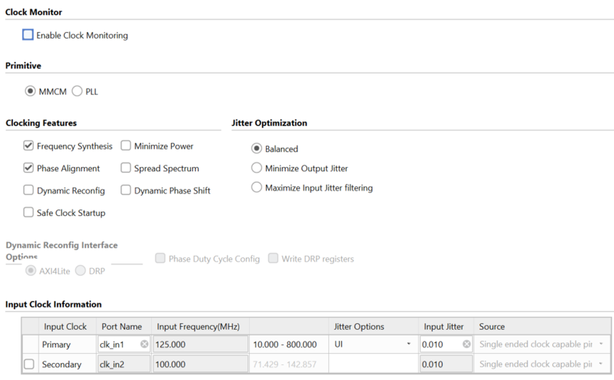
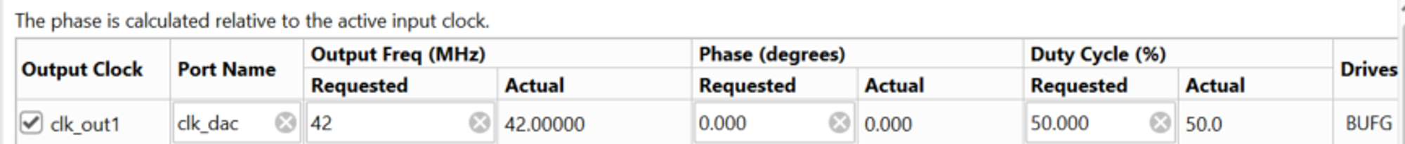
out 클럭으로 42MHz 신호(대략 24ns) 만들어줬고 이름을 clk_dac로 하겠다
synthesis 거치면
잘 합성되었음을 확인
FPGA에서 나오는 디지털 파형(14비트) 찍어보면 잘 나온다
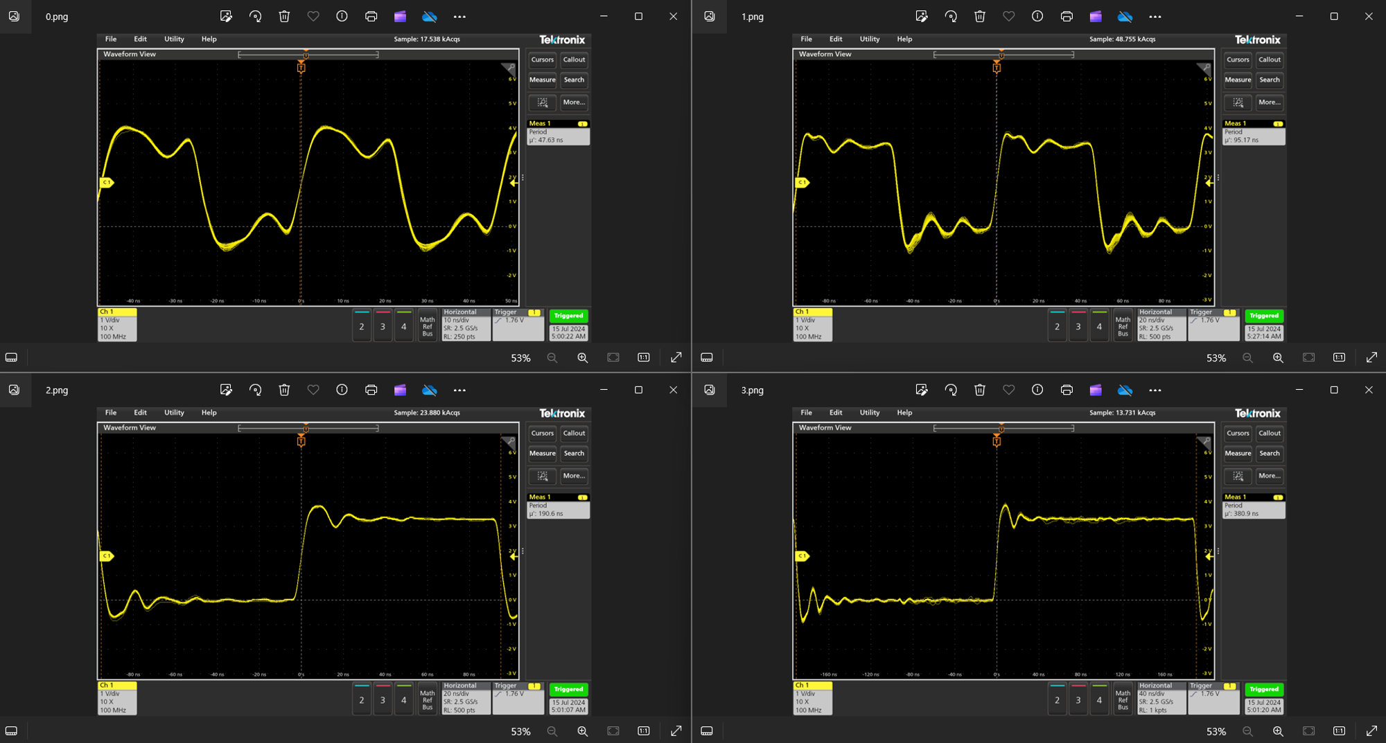
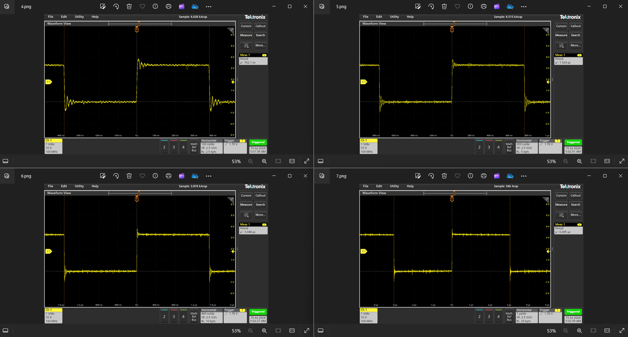
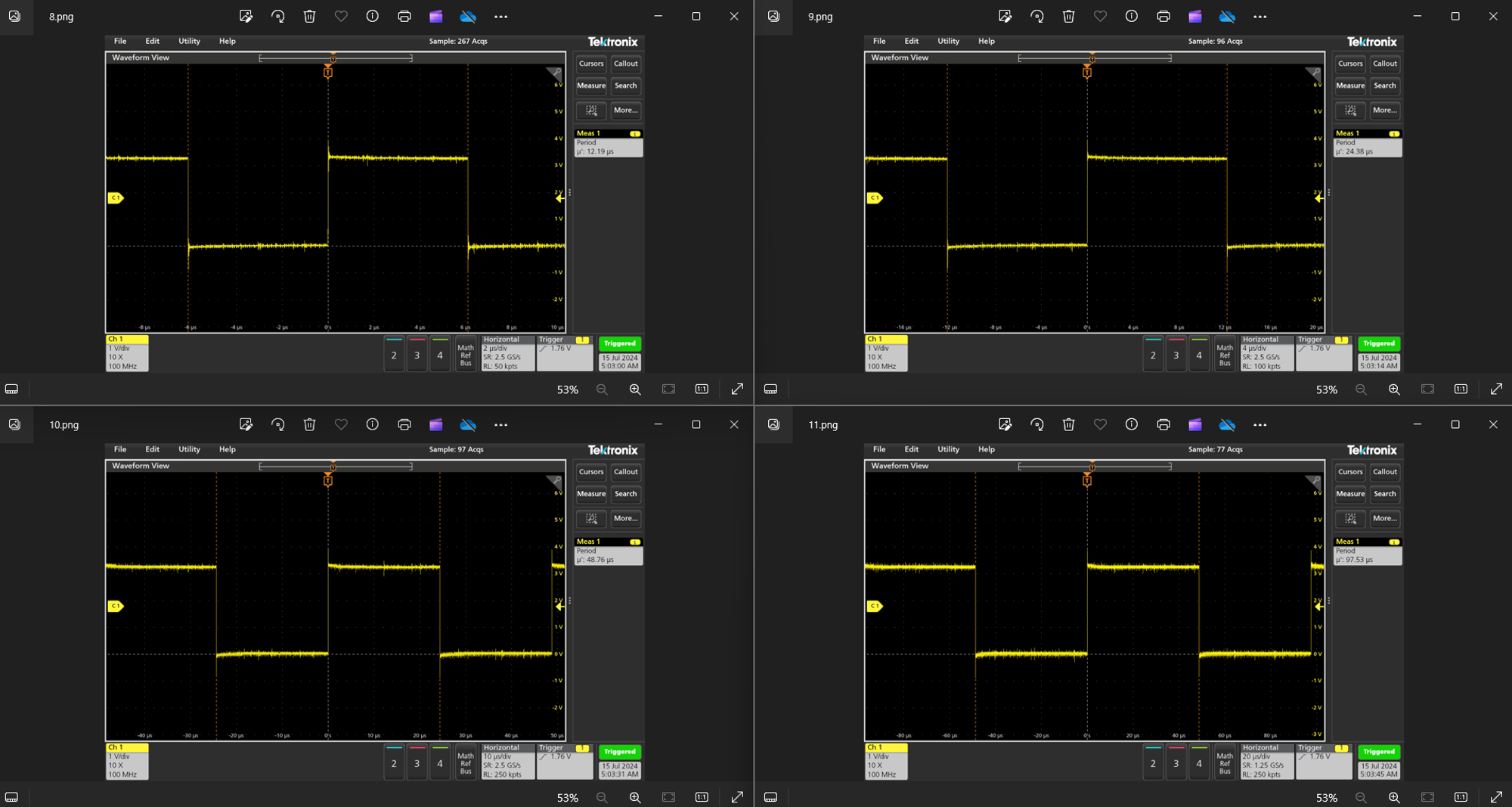
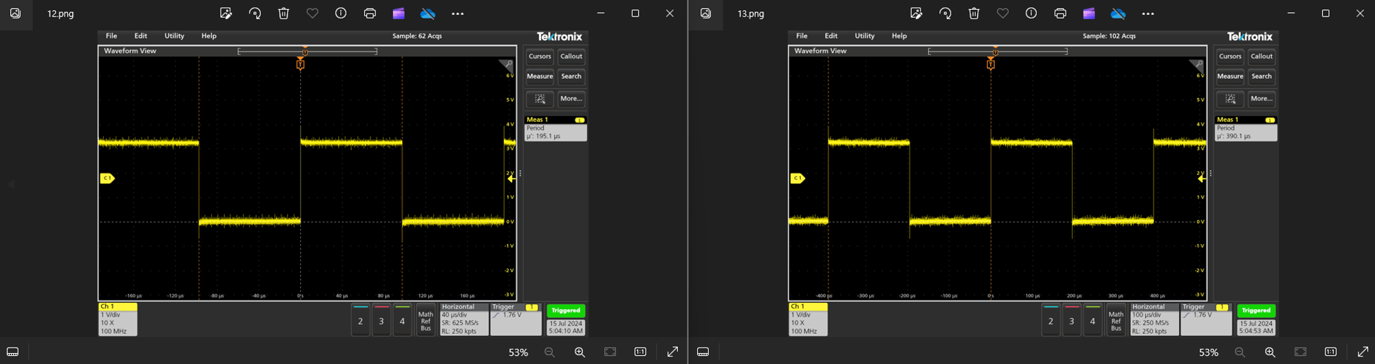
위에서부터 LSB 아래로 내려올수록 MSB(MSB로 갈수록 주기 2배씩 증가)
고주파에서 신호가 찌그러지는게 보이는데 내 생각은 오실로스코프에서 넘 고주파 신호를 못 찍나 하는 생각(단순 측정만 이렇게 되는게 아닐까 하는 생각)
DAC 모듈 내에서 DAC 역할하는 칩은 정상 동작해서
DAC 출력 전류 단자 찍어보면
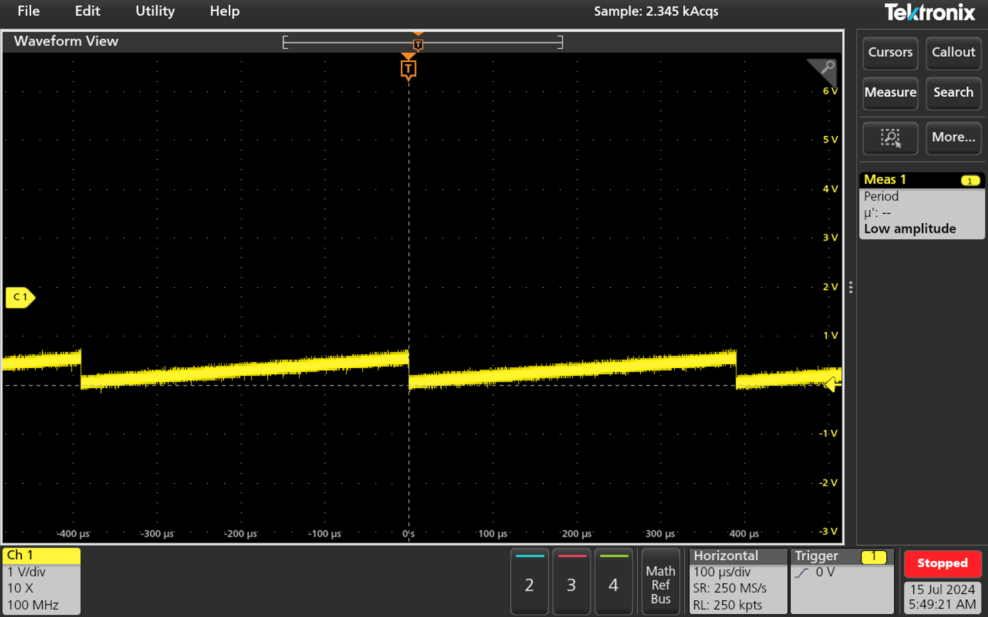
톱니파가 나옴을 확인 가능
처음에 만들고자 했던 400us안에도 나오고 있음을 확인할 수 있다.
DAC 모듈 오면 최종 출력단자 찍어볼 예정
모듈에서 출력 파형 잘 나오면 그대로 쓰면 되고
노이즈 심하면 필터 추가로 설계
----------------0804 업데이트 추가 부분-----------------
모듈 도착 완료
테스트 결과
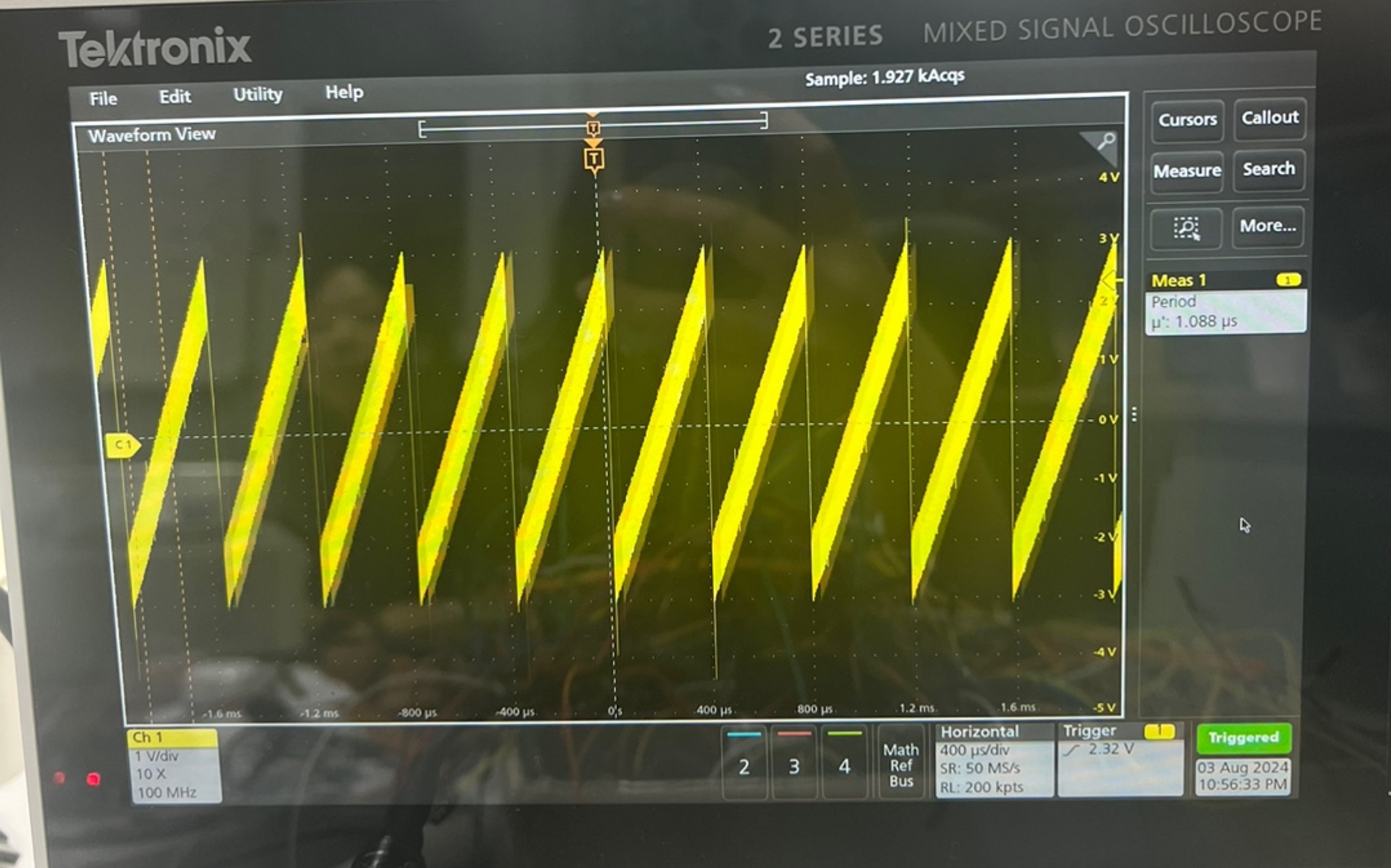
-3V에서 +3V로 나옴.
-> 왜 이런가?
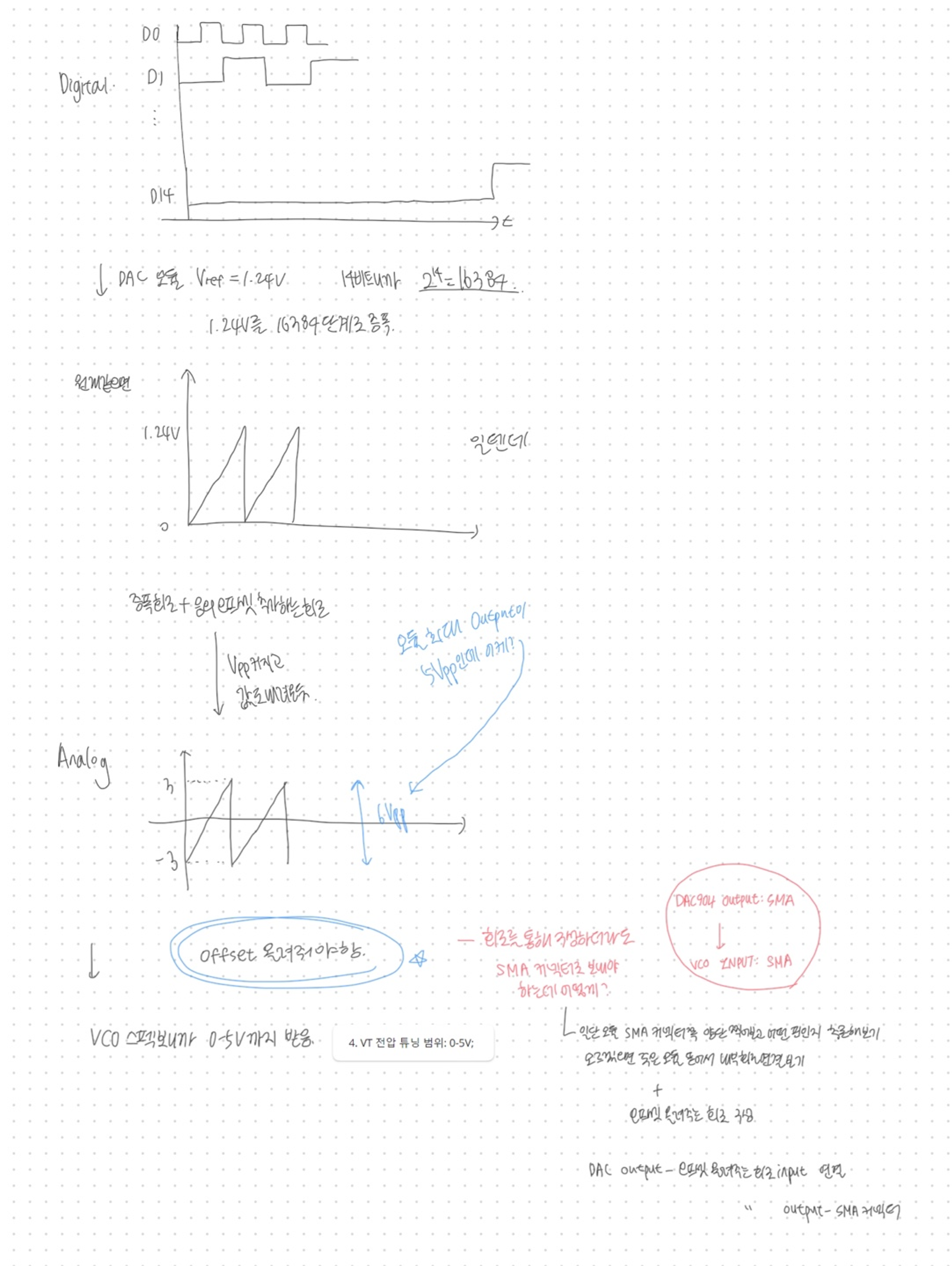
원래 0V 기준으로 출력이 나오는게 맞는데 아마 모듈 내부에서 따로 오프셋 내리는 회로가 있는듯. 모듈 내부 회로도를 몰라서 정확하게 추론할 수 없음.
아무튼 DAC 다음 단인 VCO 입력 범위가 0-5V라서 이걸 끌어올려줘야하는데..
어떻게 올리느냐?
내가 생각했을 때는 DAC 모듈의 출력을 외부 아날로그 회로로 빼내서 오프셋 올리는 회로 통과한 후 그 출력을 기판에 납땜해서 죽은 모듈의 SMA 단자를 떼와서 연결해서 최종 VCO 입력에 연결해준다.
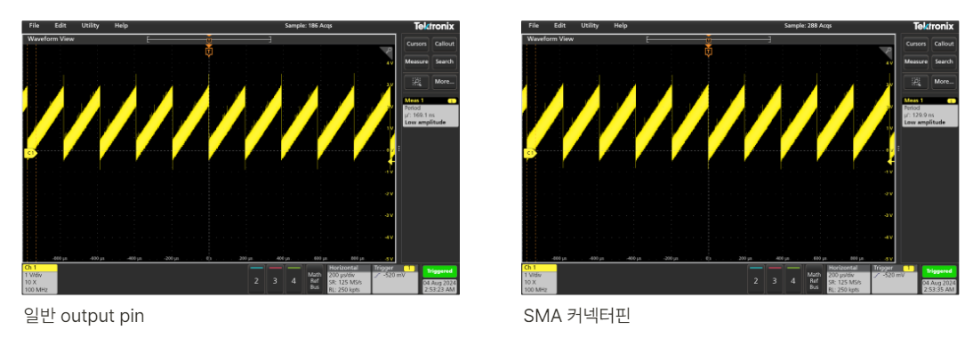
아날로그 회로 구성도 쉽지 않을 것 같고 VCO 입력에 SMA 연결한다고 해서 데이터가 그대로 출력되는가에 대한 의문도.. 무엇보다 죽은 모듈에서 SMA 커넥터가 잘 안 떼진다. 1시간동안 땜질했는데!
일단 모듈에서 SMA 주변 출력 단자 찍어봤을 때 딱 중간단자는 일반 출력핀과 같은 데이터가 나옴
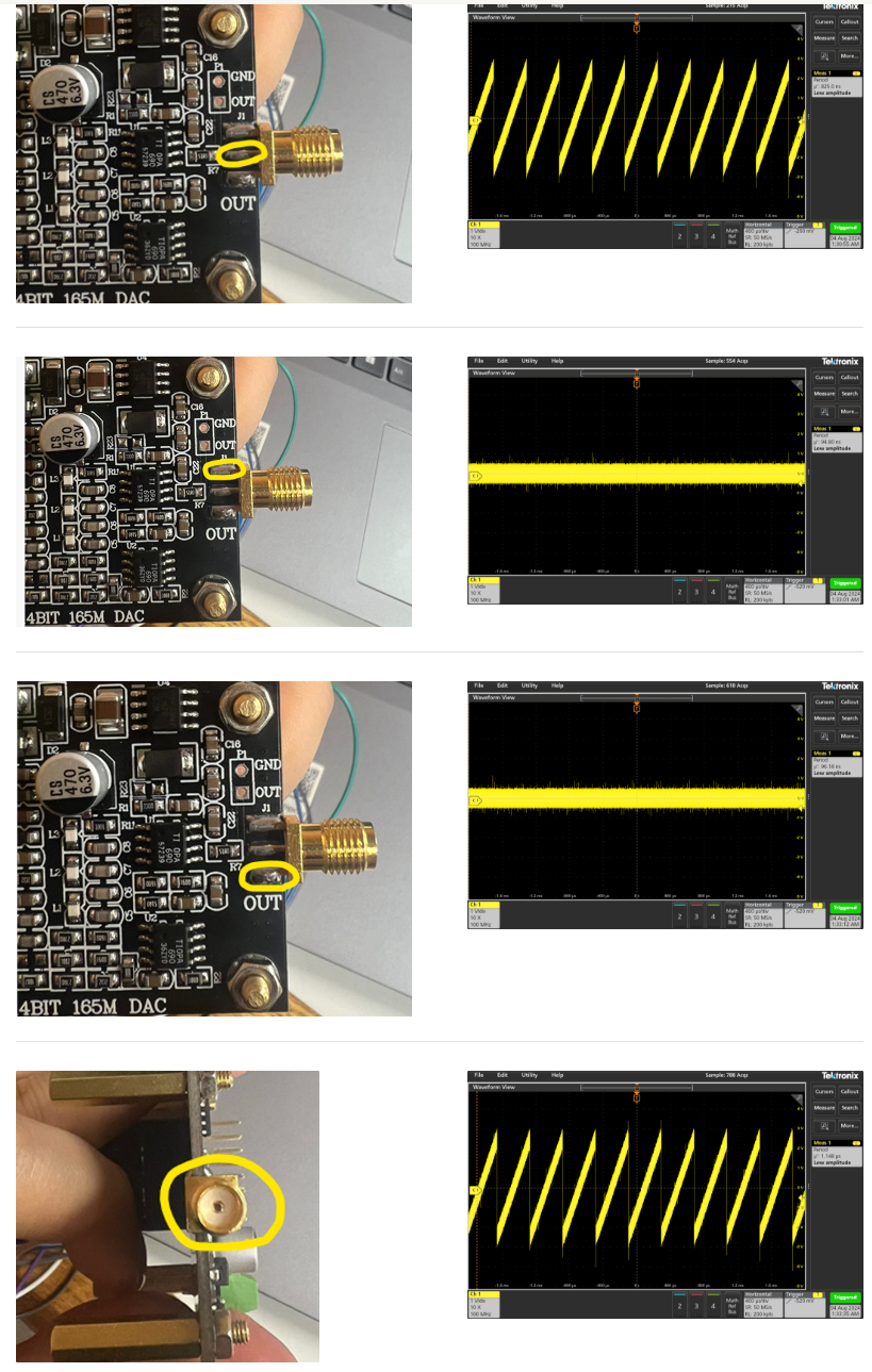
그래서 생각한점: 만약 VCO에서 0-5V까지 전압이 다 필요없다면?
내가 0-3V까지만 주면 안되나? 이 정도 파형은 생성 가능하다. 그냥 0에서부터 시작한걸 중간값부터 시작해주면 되는 것임
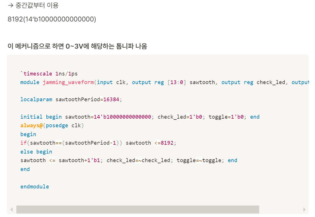
0-3V는 아주 잘 나온다
만약 5V까지 필요하다면…
offset 증폭 회로 만들어서 SMA 커넥터(죽은 모듈로부터 빼와서) 연결해서 output으로 빼줘야할 듯(위에서 만든것처럼) -단순히 SMA 커넥터 단다고 완성될 수는 없다.