목차
1. 개요
LEGv8 ISA 기반 CPU를 Verilog RTL로 설계하고 동작을 검증하였음.
CPU 구조 이해를 위해 먼저 Single Cycle CPU를 설계하고 이후 5-stage Pipeline CPU로 확장하였음.
구현 목표
- datapath 구현
- Control unit 구현
- 5-stage pipeline architecture 구현
- forwarding unit 구현
- load-use hazard stall 처리
- Branch 처리 구현
RTL 설계 이후 시뮬레이션을 통해 명령어 실행 동작을 검증하고, FPGA Synthesis 및 Implementation을 수행하여 설계한 CPU의 동작 및 timing 특성을 확인하였음.
2. 개발 환경
| 항목 | 내용 |
|---|---|
| HDL | System Verilog |
| Tool | Xilinx Vivado |
| Simulator | Vivado Simulator |
| Target FPGA | Artix-7 |
3. ISA
LEGv8 ISA 기반 instruction subset을 사용하여 CPU를 설계하였음.
| Instruction | Format | Description |
|---|---|---|
| ADD | R-format | Register addition |
| SUB | R-format | Register subtraction |
| AND | R-format | Bitwise AND |
| ORR | R-format | Bitwise OR |
| ADDI | I-format | Immediate addition |
| SUBI | I-format | Immediate subtraction |
| LDUR | D-format | Load register |
| STUR | D-format | Store register |
| B | B-format | Unconditional branch |
| CBZ | CB-format | Compare and branch if zero |
4. Single Cycle CPU
4.1 Architecture
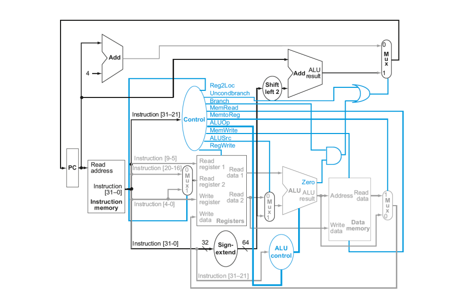
Single Cycle CPU는 모든 명령어가 하나의 clock cycle에서 실행되는 구조임.
Instruction Fetch, Decode, Execute, Memory Access, Write Back 과정이 하나의 cycle에서 수행됨.
출처 : Patterson & Hennessy, Computer Organization and Design (ARM Edition)
장점
- 구조가 단순함
- logic 구현이 비교적 쉬움
단점
- 가장 느린 instruction 기준으로 clock period가 결정됨
- instruction throughput이 낮음
Single Cycle CPU의 critical path는 PC → Instruction Memory → Register File → ALU → Data Memory → Register File write로 이어짐.
4.2 주요 모듈
Single Cycle CPU는 아래와 같은 모듈로 구성하였음.
Program Counter
현재 instruction address를 저장하는 레지스터임.
매 cycle마다 PC+4 또는 branch target address로 갱신됨.
Instruction Memory
PC 값을 입력으로 받아 해당 instruction을 출력함.
현재 설계에서는 pc[6:2]를 index로 사용하여 instruction memory에 접근함.
Register File
Rn, Rm 주소를 이용해 두 개의 register 값을 읽음.
RegWrite가 활성화되면 Rd에 결과를 저장함.
ALU
Arithmetic 및 logical 연산을 수행함.
지원 연산
- ADD
- SUB
- AND
- ORR
- LSL
CBZ instruction에서는 입력값이 0인지 판별하기 위해 zero flag를 생성함.
Data Memory
LDUR 명령어는 memory read를 수행함.
STUR 명령어는 clock edge에서 memory write를 수행함.
Sign Extension
Instruction의 immediate field를 명령어 형식에 맞게 sign-extend함.
지원 immediate
- LDUR / STUR
- B
- CBZ
- ADDI
Control Unit
Instruction opcode를 decode하여 datapath 제어 신호를 생성함.
생성되는 주요 control signal
- Reg2Loc
- Branch
- MemRead
- MemWrite
- ALUSrc
- RegWrite
4.3 Verilog code
전체 RTL 코드는 아래 GitHub repository에서 확인할 수 있음.
git주소
4.4 결과
Simulation 초기 register / memory 상태
| 유형 | 이름 | 값 | 설명 |
|---|---|---|---|
| Register | x1 | 2 | ALU 연산 operand |
| Register | x2 | 3 | ALU 연산 operand |
| Register | x10 | 11 | LDUR/STUR 명령어 base address |
| Register | x11 | 0 | CBZ branch 조건 확인 |
| Memory | memory[12] | 99 | LDUR load 결과 확인용 값 |
Test Program
CPU 동작 검증을 위해 다음 instruction sequence를 사용하였음.
| PC | Instruction | Description |
|---|---|---|
| 0 | ADD x3,x1,x2 | ALU addition test |
| 1 | SUB x4,x1,x2 | ALU subtraction test |
| 2 | LDUR x9,[x10,#1] | memory read |
| 3 | STUR x4,[x10,#1] | memory write |
| 4 | LDUR x9,[x10,#1] | memory write result check |
| 5 | AND x5,x3,x4 | bitwise AND |
| 6 | ORR x6,x3,x4 | bitwise OR |
| 7 | ADDI x22,x22,#1 | immediate addition |
| 8 | LSL x10,x22,#3 | shift operation |
| 9 | CBZ x11,#2 | conditional branch |
| 10 | LSL x10,x22,#3 | branch fall-through |
| 11 | B -1 | infinite loop (halt) |
Simulation 결과
- PC 동작

PC 값이 매 cycle마다 4씩 증가하며 instruction fetch가 정상적으로 수행됨을 확인하였음.
- Instruction execution waveform
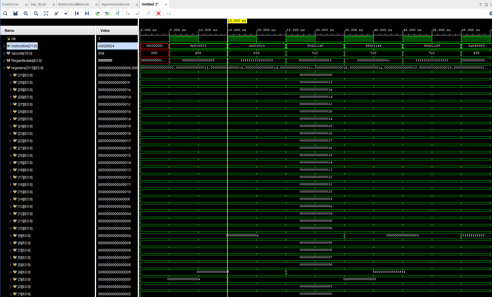
Test program이 순차적으로 실행되며 각 instruction 실행 결과가 예상한 register 값과 일치함을 확인하였음.
4.5 Synthesis 및 Implementation 결과
Single Cycle CPU의 timing 특성을 확인하기 위해 두 가지 clock constraint 조건에서 Implementation을 수행하였음.
| Clock Period | Frequency | Result |
|---|---|---|
| 10 ns | 100 MHz | Timing violation |
| 12.5 ns | 80 MHz | Timing closure |
4.5.1 100 MHz (10 ns)
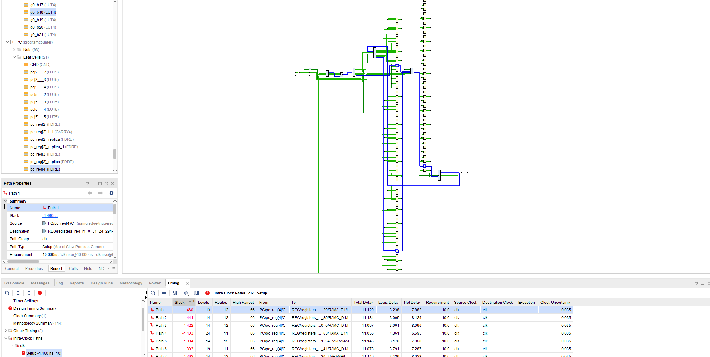
100 MHz constraint 조건에서 Implementation을 수행하였으나 timing violation이 발생하였음.
| Metric | Result |
|---|---|
| WNS | -1.460 ns |
| TNS | -155.375 ns |

Critical path를 확인한 결과 Single Cycle 구조에서는 instruction execution이 하나의 cycle에서 수행되기 때문에 logic 및 routing 지연이 길어 timing을 만족하지 못하였음.
4.5.2 80 MHz (12.5 ns)
12.5 ns constraint 조건에서 Implementation을 수행한 결과 timing closure를 확인하였음.
| Metric | Result |
|---|---|
| WNS | 0.103 ns |
| TNS | 0 ns |

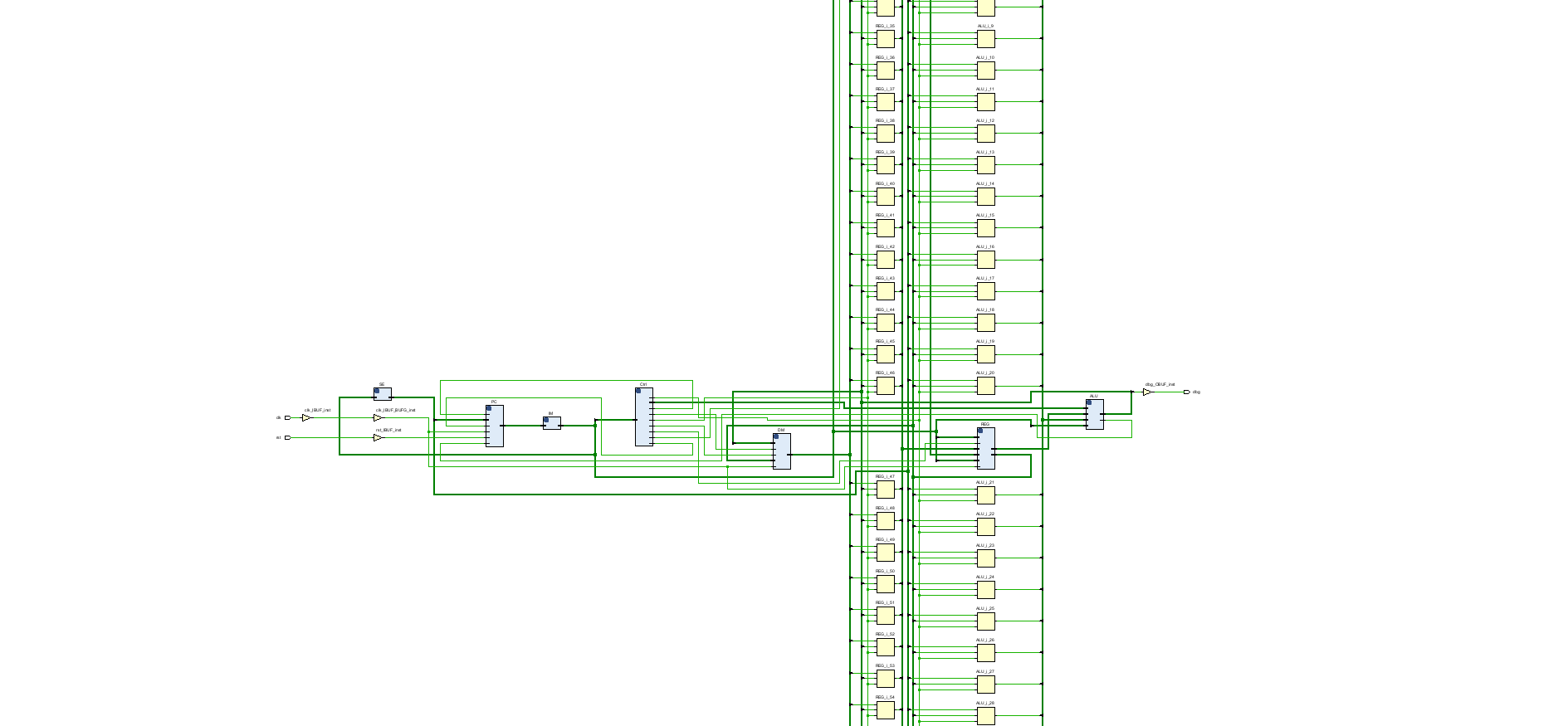
Schematic
생성된 회로 구조를 통해 RTL에서 설계한 datapath 구조가
FPGA logic resource(LUT, register 등)로 정상적으로 매핑된 것을 확인하였음.
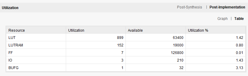
Resource Utilization
| Resource | Used | Available | Utilization (%) |
|---|---|---|---|
| LUT | 899 | 63400 | 1.42 |
| LUTRAM | 152 | 19000 | 0.80 |
| FF | 7 | 126800 | 0.01 |
| IO | 3 | 210 | 1.43 |
| BUFG | 1 | 32 | 3.13 |
Artix-7 FPGA 기준으로 LUT 1.42% 수준의 자원을 사용하여 비교적 작은 규모의 CPU임을 확인할 수 있음.
5. Pipeline CPU
5.1 Architecture
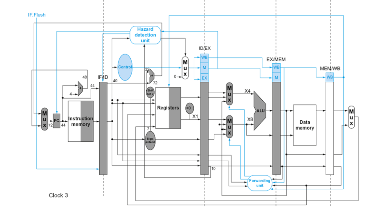
Pipeline CPU는 명령어 실행을 여러 단계로 분리하여 instruction throughput을 향상시키는 구조임.
설계한 pipeline은 다음 5개의 stage로 구성됨.
| Stage | 기능 |
|---|---|
| IF | Instruction Fetch |
| ID | Instruction Decode |
| EX | ALU Execute |
| MEM | Memory Access |
| WB | Write Back |
각 stage 사이에는 다음 pipeline register가 존재함.
- IF / ID
- ID / EX
- EX / MEM
- MEM / WB
출처 : Patterson & Hennessy, Computer Organization and Design (ARM Edition)
5.2 주요 모듈
Pipeline CPU에서는 instruction execution이 여러 stage로 분리되기 때문에
instruction dependency로 인해 hazard가 발생할 수 있음.
이를 해결하기 위해 다음과 같은 제어 로직을 구현하였음.
Forwarding Unit
Data hazard를 해결하기 위해 forwarding 경로를 구현하였음.
Forwarding Unit은 EX stage에서 사용되는 source register와
EX/MEM, MEM/WB pipeline register의 destination register를 비교하여
필요한 경우 forwarding 경로를 선택하도록 설계하였음.
Forwarding 경로
- EX/MEM → EX forwarding
- MEM/WB → EX forwarding
이를 통해 register write 이전의 값을 바로 ALU 입력으로 전달하여
pipeline stall 없이 연산을 수행할 수 있도록 하였음.
Hazard Detection Unit
Load instruction 이후 바로 해당 register를 사용하는 경우
forwarding만으로 해결할 수 없는 load-use hazard가 발생함.
이를 해결하기 위해 Hazard Detection Unit을 구현하였음.
Hazard Detection Unit은
- ID stage의 source register
- EX stage의 load instruction destination register
를 비교하여 dependency가 발생할 경우
- PC write disable
- IF/ID pipeline register stall
- control signal bubble 삽입
을 수행하도록 설계하였음.
이를 통해 pipeline stall을 발생시켜 올바른 instruction 실행 순서를 유지하도록 하였음.
Branch Control Logic
Branch instruction 실행 시 잘못 fetch된 instruction이 pipeline에 존재할 수 있음.
이를 해결하기 위해 branch 발생 시 pipeline flush를 적용하였음.
Branch 조건이 만족될 경우
- IF/ID pipeline register flush
- PC를 branch target address로 변경하도록 설계하여 control hazard를 처리하였음.
5.3 Verilog code
전체 RTL 코드는 아래 GitHub repository에서 확인할 수 있음.
git주소
5.4 Simulation 결과
Simulation 초기 register / memory 상태
| 유형 | 레지스터 | 값 | Description |
|---|---|---|---|
| Register | x1 | 2 | ALU 연산 operand |
| Register | x2 | 3 | ALU 연산 operand |
| Register | x10 | 11 | LDUR 명령어의 base address |
| Register | x11 | 0 | CBZ branch 조건 확인 |
| Register | x15 | 16 | CBZ not-taken 테스트 |
| Memory | memory[12] | 99 | LDUR load 결과 확인용 값 |
Test Program
Pipeline CPU 동작 검증을 위해 다음 instruction sequence를 사용하였음.
| 순번 | Instruction | Description |
|---|---|---|
| 0 | ADD x3,x1,x2 | ALU addition |
| 1 | SUB x4,x3,x1 | data dependency test |
| 2 | AND x5,x4,x3 | forwarding test |
| 3 | ORR x6,x5,x4 | forwarding test |
| 4 | LDUR x9,[x10,#1] | memory read |
| 5 | ADD x12,x9,x1 | load-use hazard test |
| 6 | SUB x13,x12,x2 | forwarding after stall |
| 7 | SUB x14,x1,x1 | branch condition |
| 8 | CBZ x14,#2 | branch taken test |
| 9 | ADDI x20,x20,#1 | flushed instruction |
| 10 | ADDI x21,x21,#1 | branch target execution |
| 11 | ADDI x15,x15,#1 | arithmetic operation |
| 12 | CBZ x15,#2 | branch not taken |
| 13 | ADDI x22,x22,#1 | sequential execution |
| 14 | SUB x16,x2,x2 | zero result generation |
| 15 | CBZ x16,#2 | branch taken |
| 16 | ADDI x23,x23,#1 | flushed instruction |
| 17 | ADDI x24,x24,#1 | branch target execution |
| 18 | B #0 | infinite loop (halt) |
- Data Hazard (Forwarding)
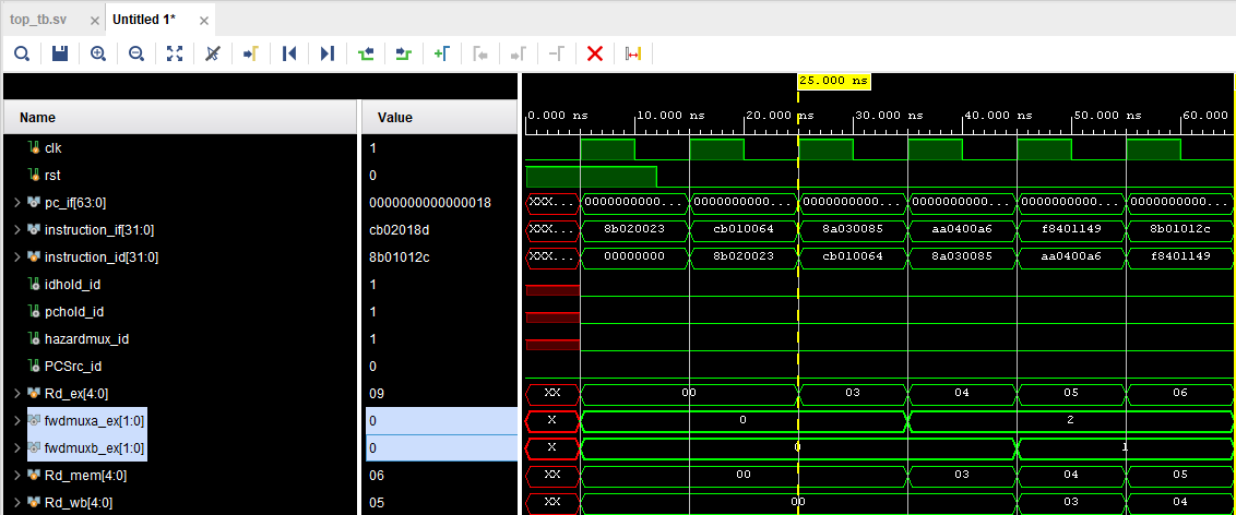
Data hazard 발생 시, Forwarding Mux의 값이 변함
- Data Hazard (Load-use stall)
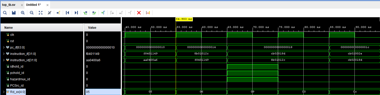
Load-use hazard 발생 시, pc_if, instruction_id가 멈춤.
-
Control Hazard (Branch + Pipeline Flush)
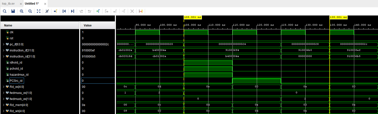
Control hazard 발생 시, instruction_id가 0으로 bubble이 삽입됨. -
Register write result
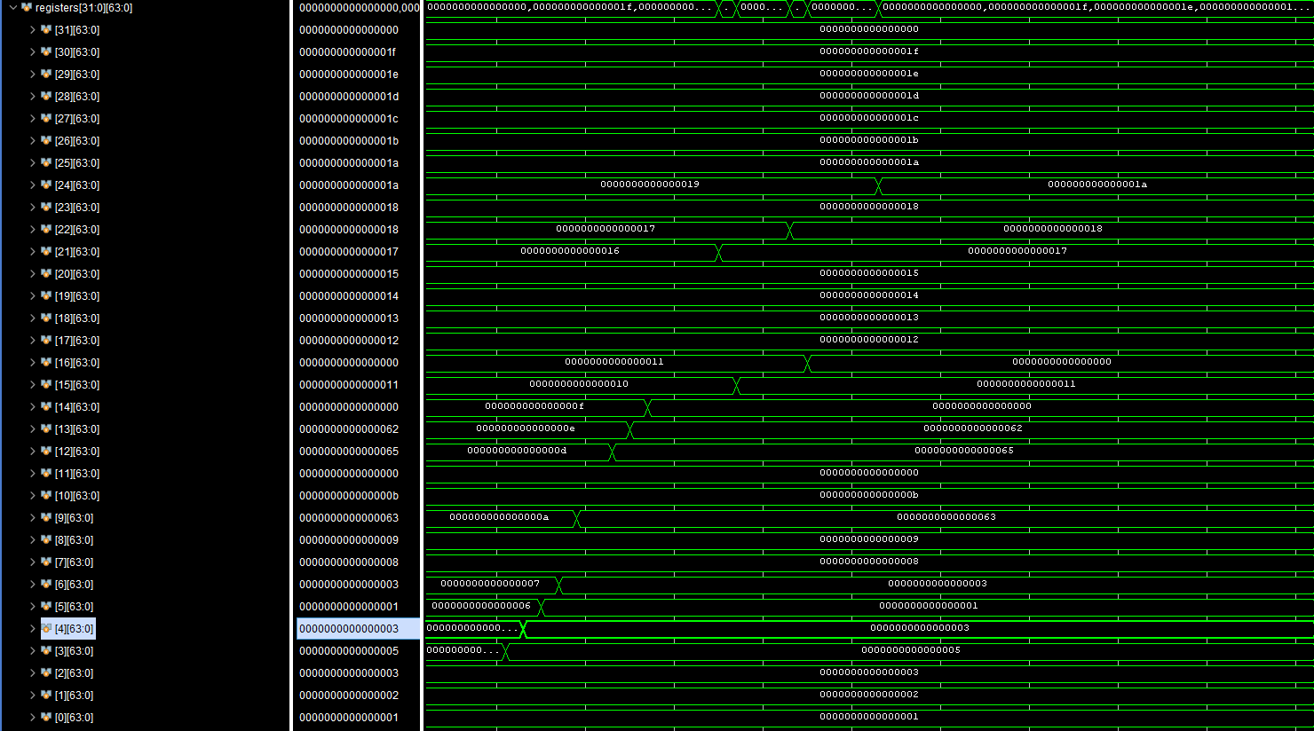
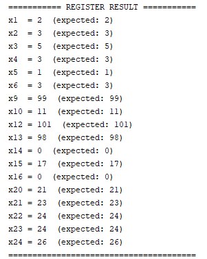
최종적으로 register에 저장되는 값은 예상 결과와 같음
5.5 Synthesis 및 Implementation 결과
Pipeline CPU의 timing 특성을 확인하기 위해 세 가지 clock constraint 조건에서 Implementation을 수행하였음.
| Clock Period | Frequency | Result |
|---|---|---|
| 5 ns | 200 MHz | Timing violation |
| 8.696 ns | 115 MHz | Timing violation |
| 8.85 ns | 112.87 MHz | Timing closure |
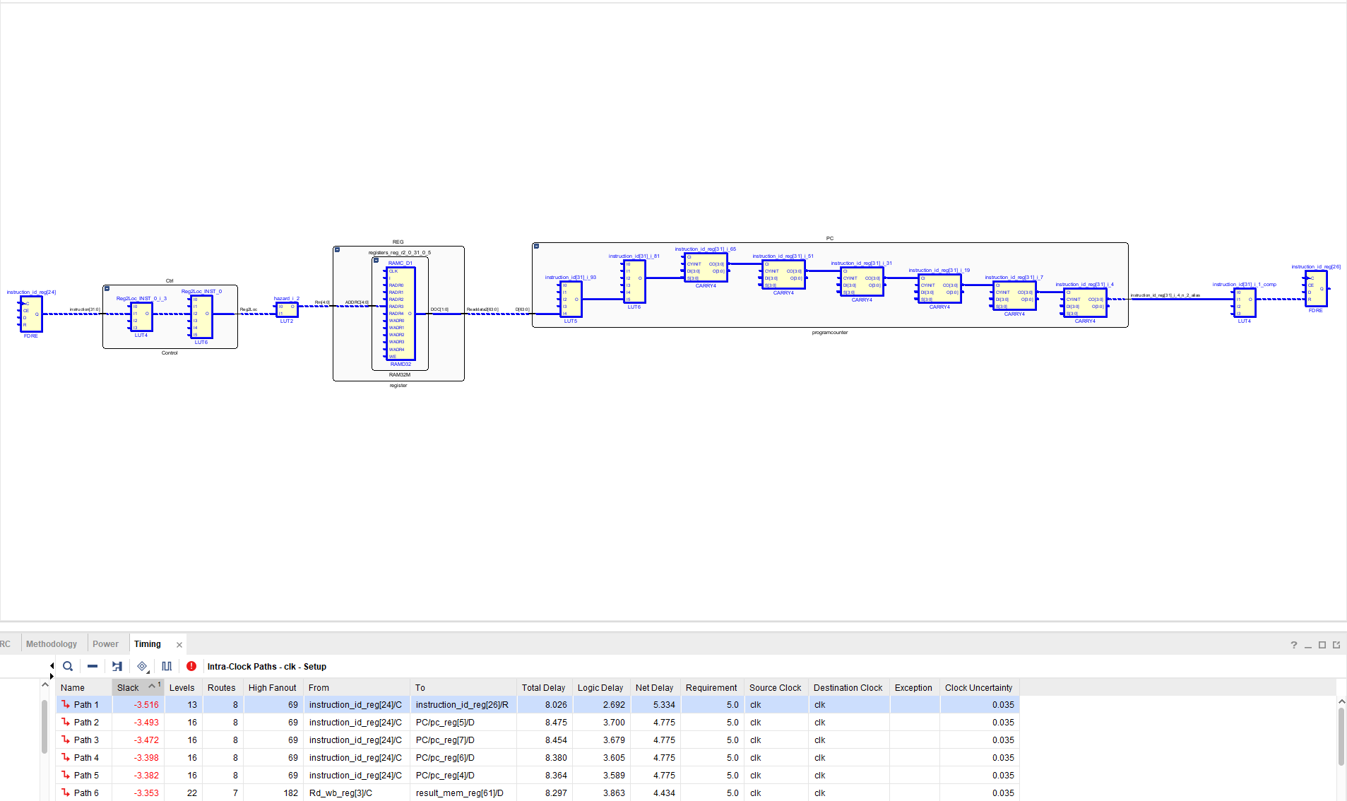
5.5.1 200 MHz (5 ns)
200 MHz constraint 조건에서 Implementation을 수행하였으나 timing violation이 발생하였음.
| Metric | Result |
|---|---|
| WNS | -3.516 ns |
| TNS | -346.881 ns |

Critical path를 확인한 결과 높은 clock frequency 조건에서
pipeline register 간 datapath 지연을 만족하지 못하였음.
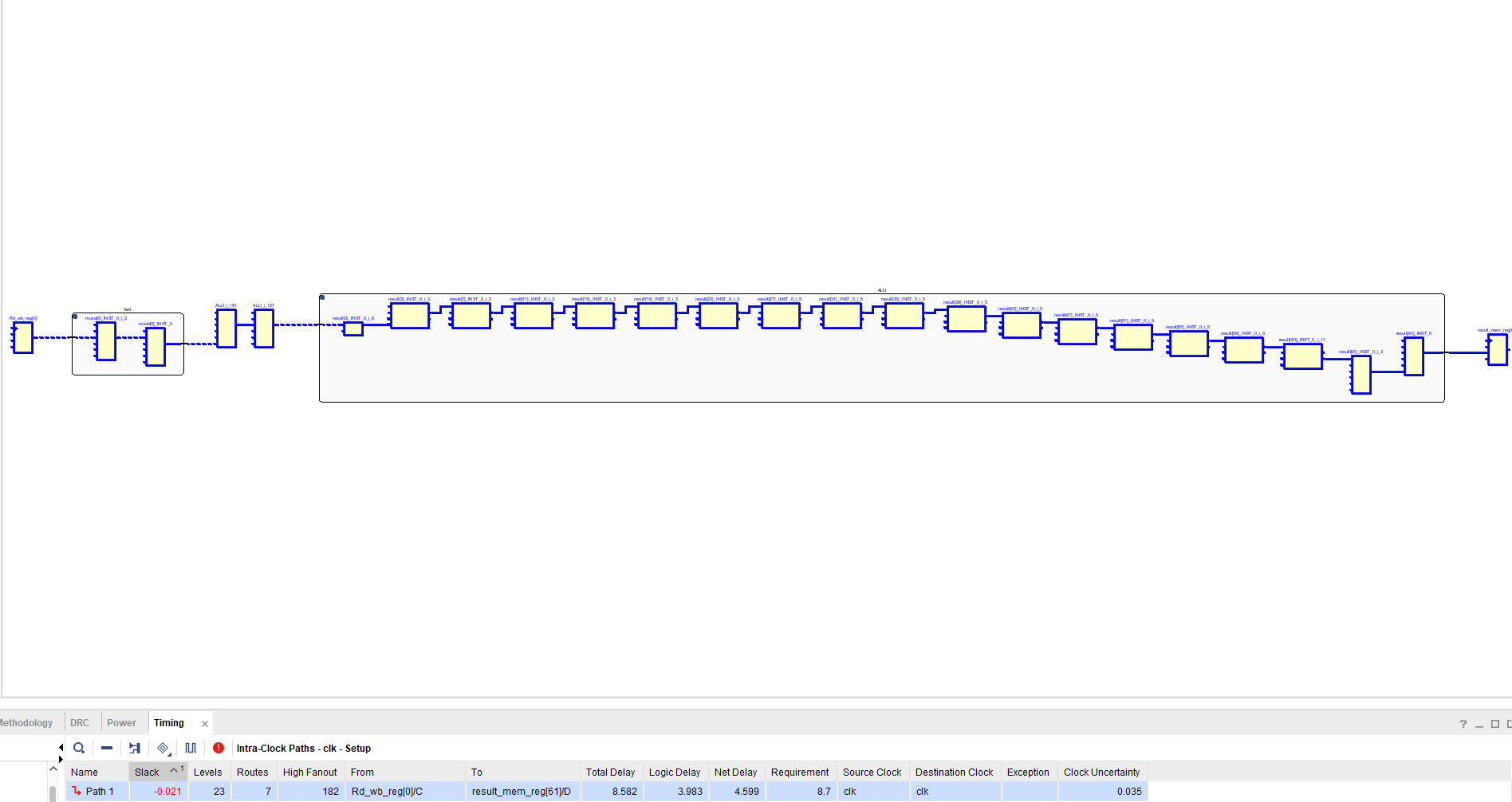
5.5.2 115 MHz (8.696 ns)
115 MHz constraint 조건에서 Implementation을 수행하였으나
timing violation이 발생하였음.
| Metric | Result |
|---|---|
| WNS | -0.021 ns |
| TNS | -0.021 ns |

8.86 ns 조건과 비교했을 때 timing margin이 부족하여
timing closure에 실패하였음.
5.5.3 112.87 MHz (8.85 ns)
8.86 ns constraint 조건에서 Implementation을 수행한 결과
timing closure를 확인하였음.
| Metric | Result |
|---|---|
| WNS | 0.034 ns |
| TNS | 0 ns |

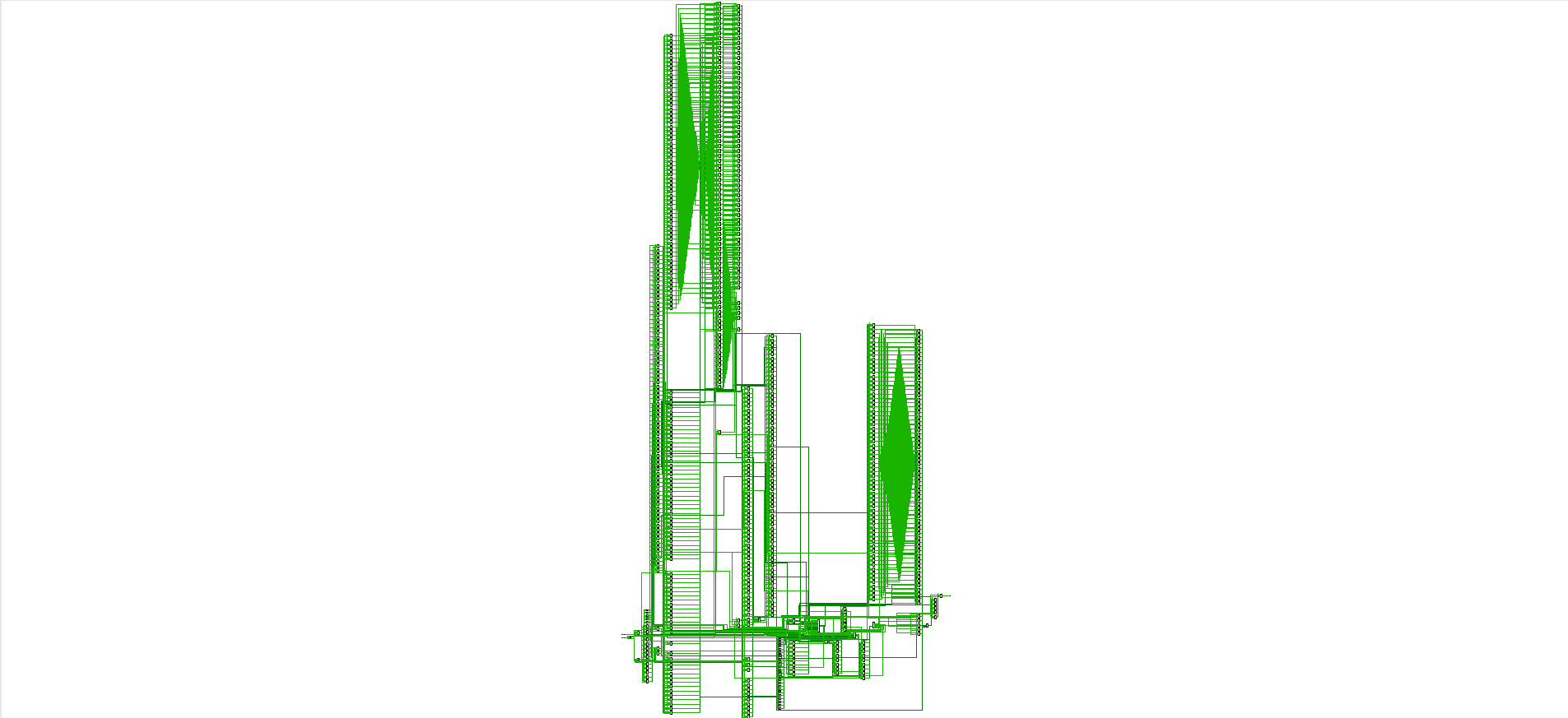
Schematic
생성된 회로 구조를 통해 RTL에서 설계한 datapath 구조가
FPGA logic resource(LUT, register 등)로 정상적으로 매핑된 것을 확인하였음.
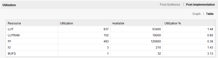
Resource Utilization
| Resource | Used | Available | Utilization (%) |
|---|---|---|---|
| LUT | 937 | 63400 | 1.48 |
| LUTRAM | 152 | 19000 | 0.80 |
| FF | 483 | 126800 | 0.38 |
| IO | 3 | 210 | 1.43 |
| BUFG | 1 | 32 | 3.13 |
Artix-7 FPGA 기준으로 LUT 1.48% 수준의 자원만 사용하여 비교적 작은 규모의 CPU 설계임을 확인하였음.
6. 성능 비교
Single Cycle/Pipeline CPU 결과표
| Metric | Single Cycle CPU | Pipeline CPU | Change |
|---|---|---|---|
| Max Frequency | 80 MHz | 112.87 MHz | +41.1 % |
| Clock Period | 12.5 ns | 8.85 ns | -29.2 % |
| LUT | 899 | 937 | +4.2 % |
| FF | 7 | 483 | +6800 % |
| LUTRAM | 152 | 152 | 0 % |
| BUFG | 1 | 1 | 0 % |
-
Pipeline 구조를 적용하여 datapath의 critical path가 감소하였고, 그 결과 최대 동작 주파수는 80 MHz → 112.87 MHz (약 1.41×)로 향상되었음.
-
Pipeline register 추가로 FF 사용량은 증가하였으나, LUT 사용량 증가는 4.2 % 수준으로 비교적 작은 수준에 그쳤음.