목차
- 개요
- 개발환경
- System Architecture
- Sobel IP Architecture
- Latency and Throughput
- Implementation Issue
- Test Image & Result
- Implementation Results
- Summary
- 결론
1. 개요
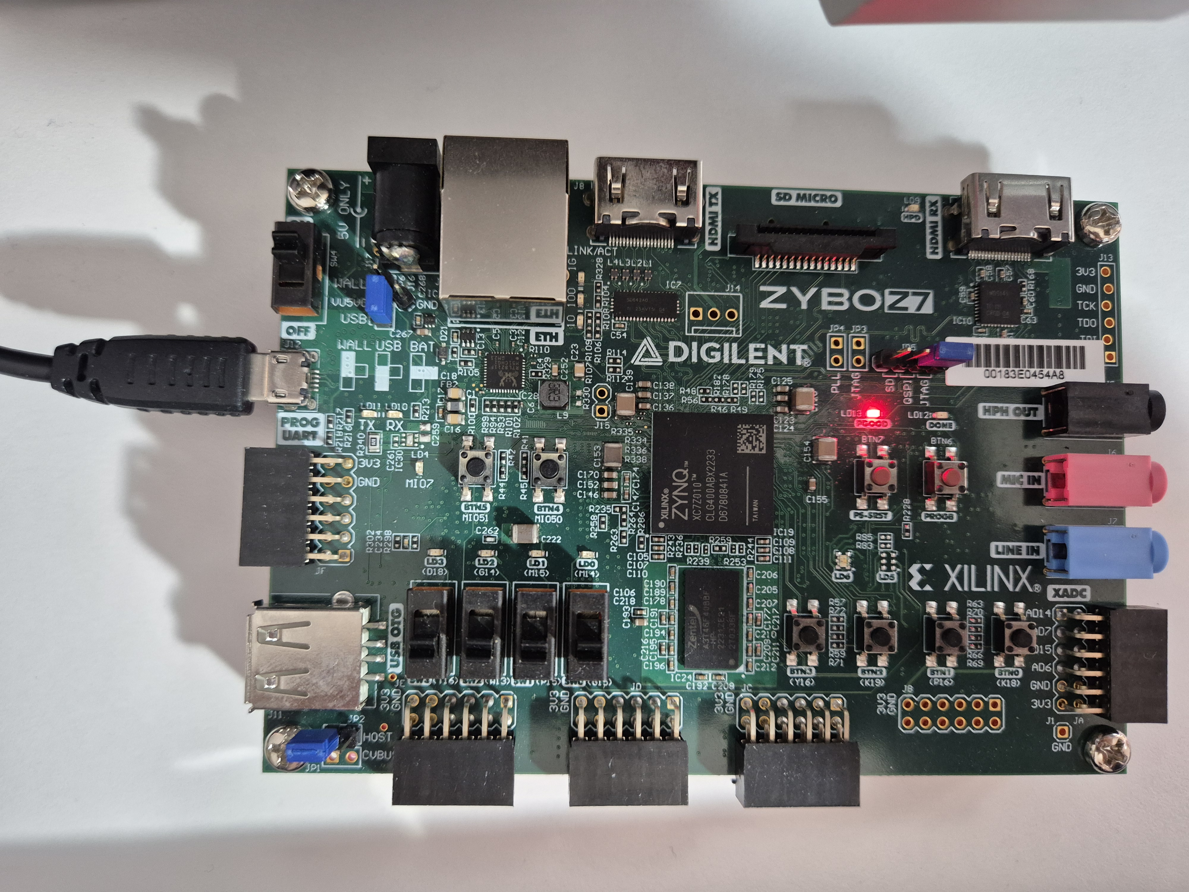
Zybo Z7-10 보드에서 AXI-DMA와 AXI4-Stream 인터페이스를 이용한 Sobel edge detection 이미지 처리 시스템을 구현하였습니다.
Zynq PS에서 DDR 메모리에 저장된 이미지를 DMA를 통해 PL로 전달하고, PL에 구현한 Sobel IP에서 3×3 sliding window 기반 edge detection을 수행한 뒤 결과를 다시 DDR에 저장하는 구조로 설계하였습니다.
2. 개발환경
| 항목 | 설명 |
|---|---|
| Board | Zybo Z7-10 |
| Device | xc7z010clg400-1 |
| HDL | Verilog |
| Tool | Vivado / Vitis |
| Interface | AXI4-Stream |
| Data Transfer | AXI DMA |
| Processor | Zynq-7000 Processing System |
| Image Format | Grayscale 8-bit |
| Resolution | 640 × 480 |
| Verification | Python reference model |
3. System Architecture
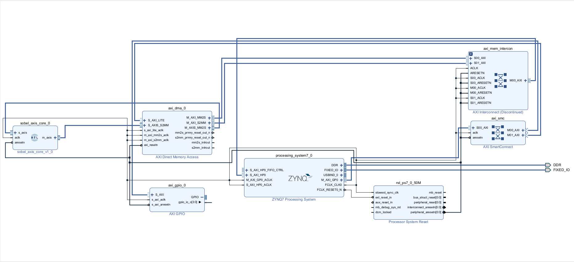
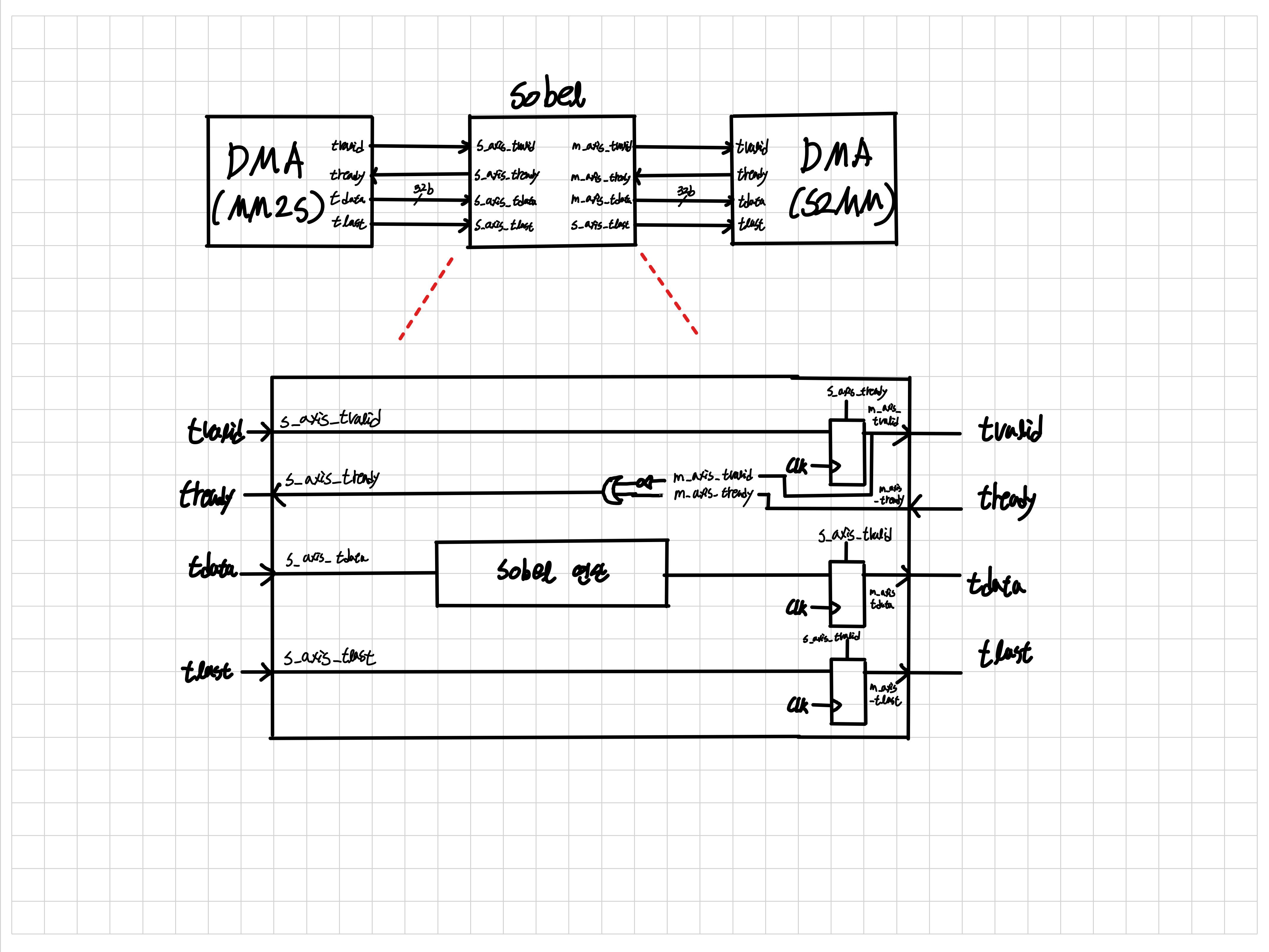
전체 데이터 흐름
img_header.h -> PS -> DDR
→ AXI DMA (MM2S)
→ AXI4-Stream
→ Sobel IP
→ AXI4-Stream
→ AXI DMA (S2MM)
→ DDR
→ PS → UART → PC -> img_result.png
각 블록의 역할
-
PS (Processing System)
DDR 메모리 접근 및 DMA 제어
DATA READ/WRITE는 little endian방식 -
AXI DMA
DDR ↔ PL 간 이미지 데이터 전송 // Word(4byte) -
Sobel IP
AXI4-Stream 기반 실시간 Sobel 연산 수행
4. Sobel IP Architecture
Sobel 연산을 수행하기 위해 아래의 구조로 구현하였습니다.
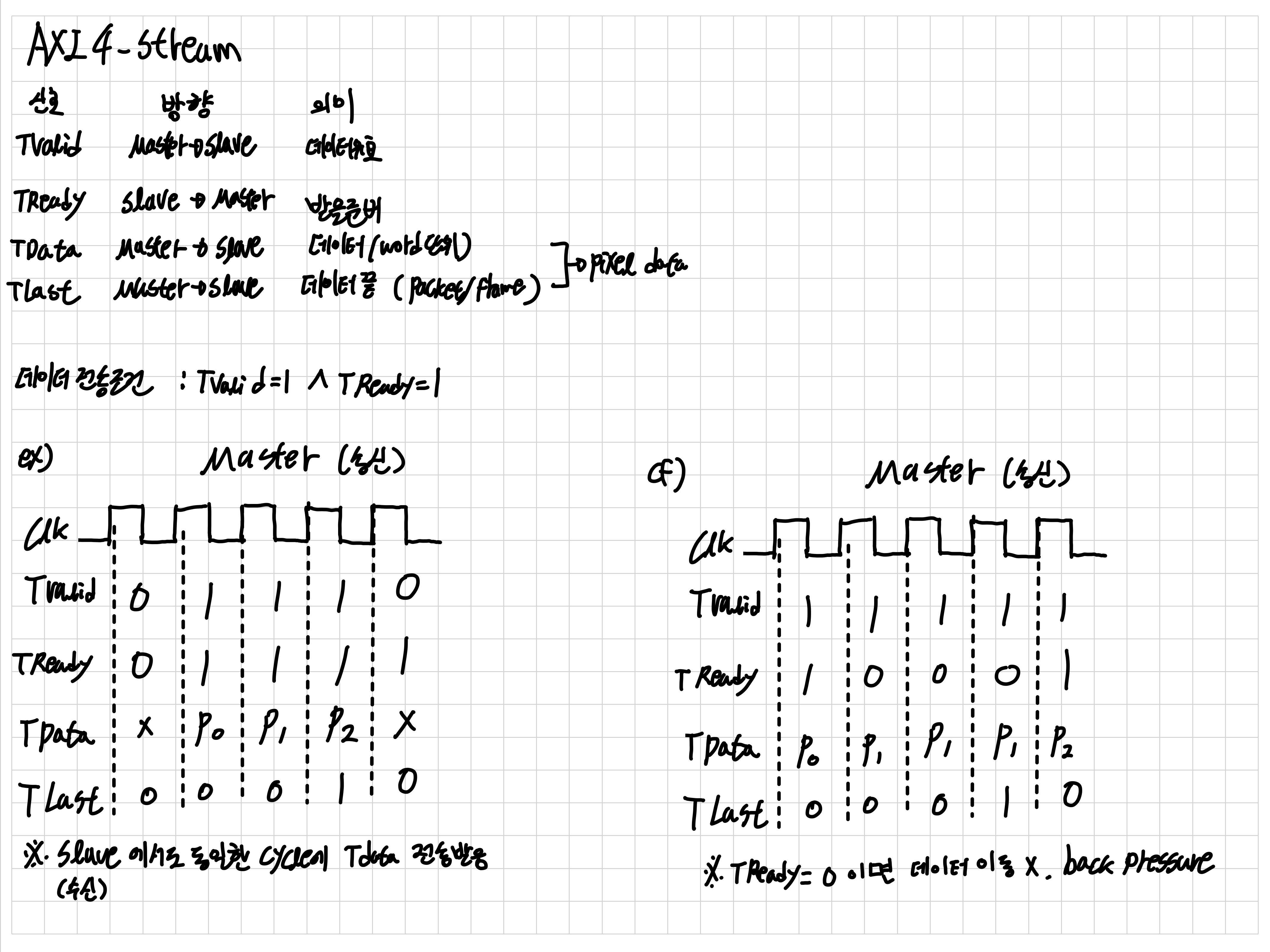
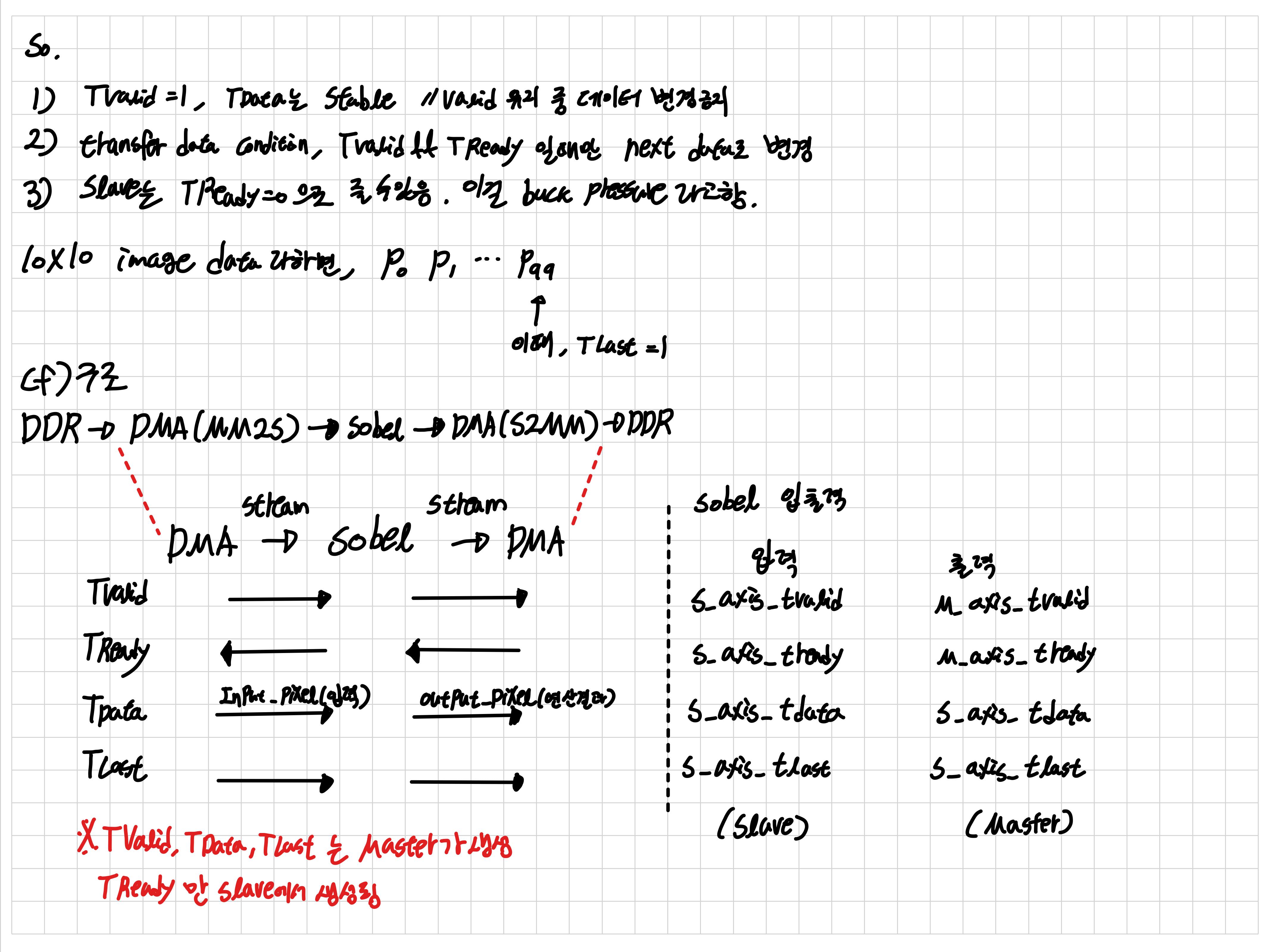
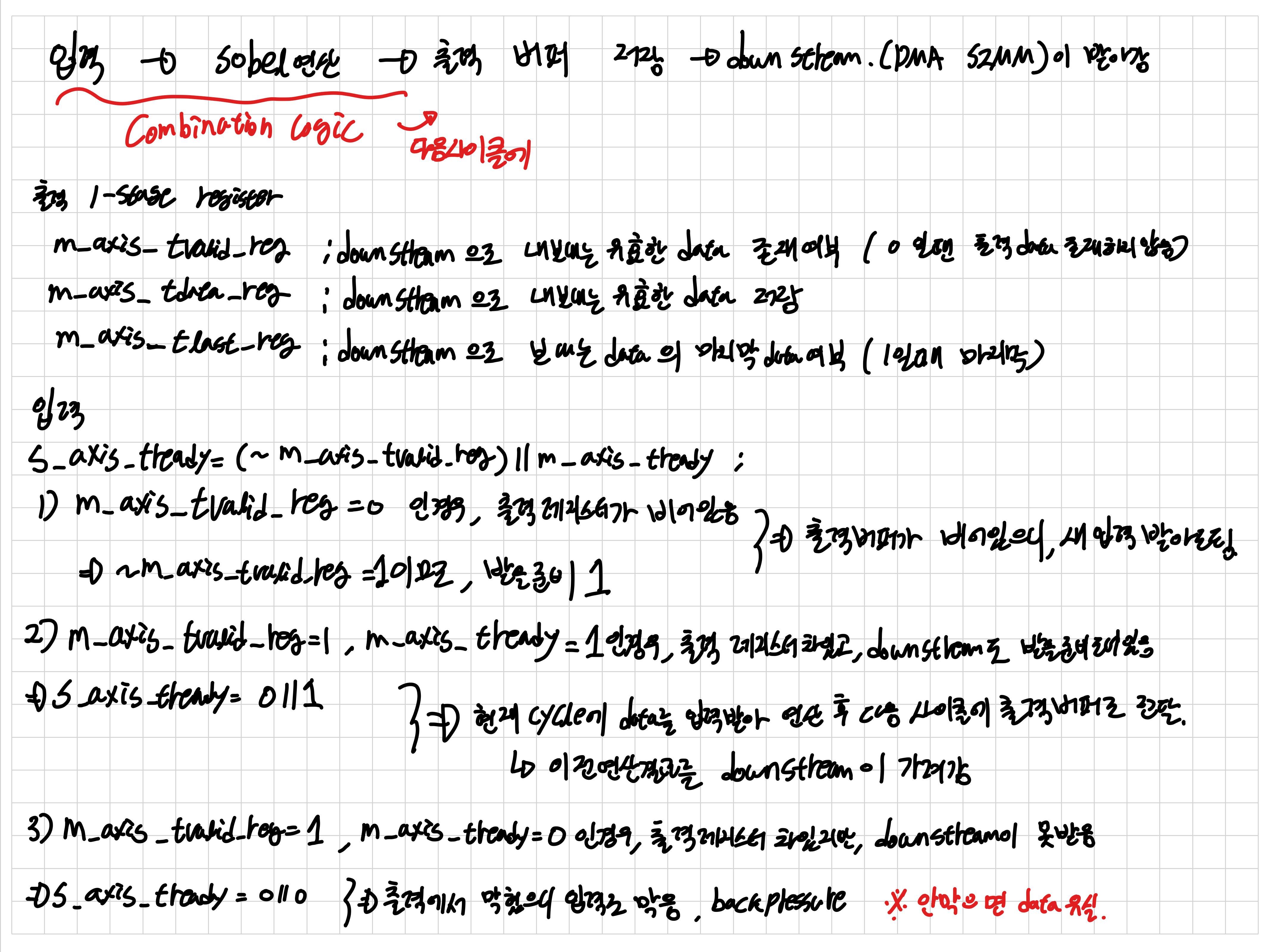
- AXI4-Stream
- Line Buffer & Window
- Sobel Convolution, Magnitude
AXI4-Stream 인터페이스 기반으로 설계하여
DMA와 직접 연결될 수 있도록 구성하였습니다.
또한 AXI-Stream 인터페이스와 DMA 전송 길이를 고려하여
stream 길이가 유지되도록 border 영역을 padding 방식으로 처리하였습니다.
4-1 AXI4-Stream
4-2 Line Buffer & Window
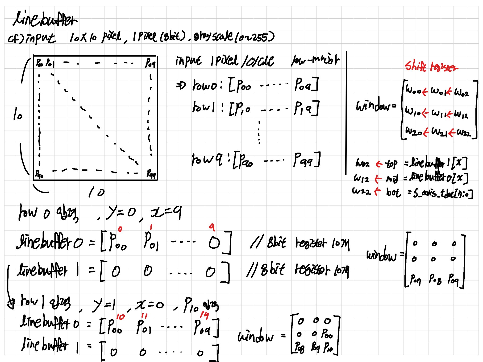
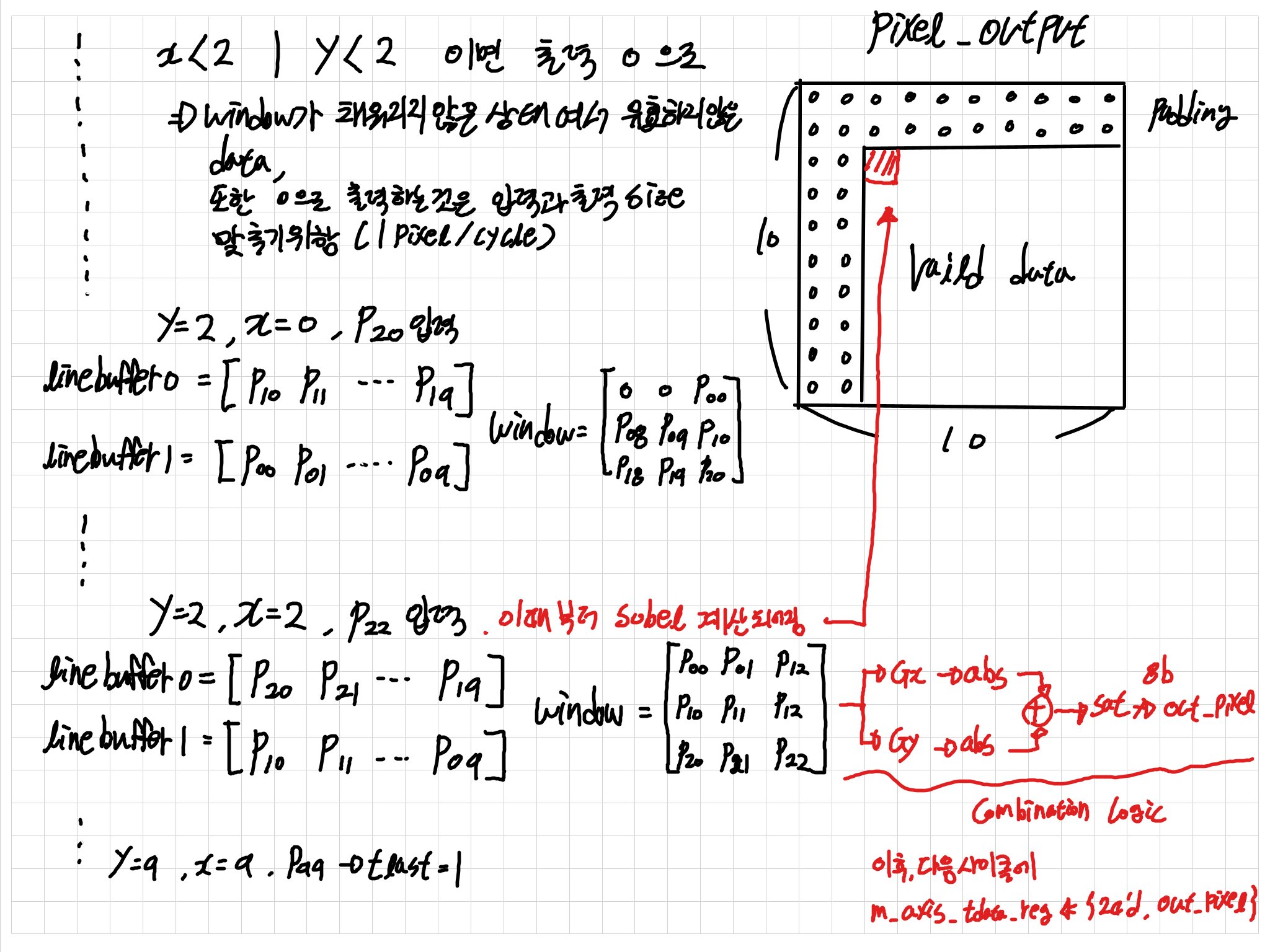
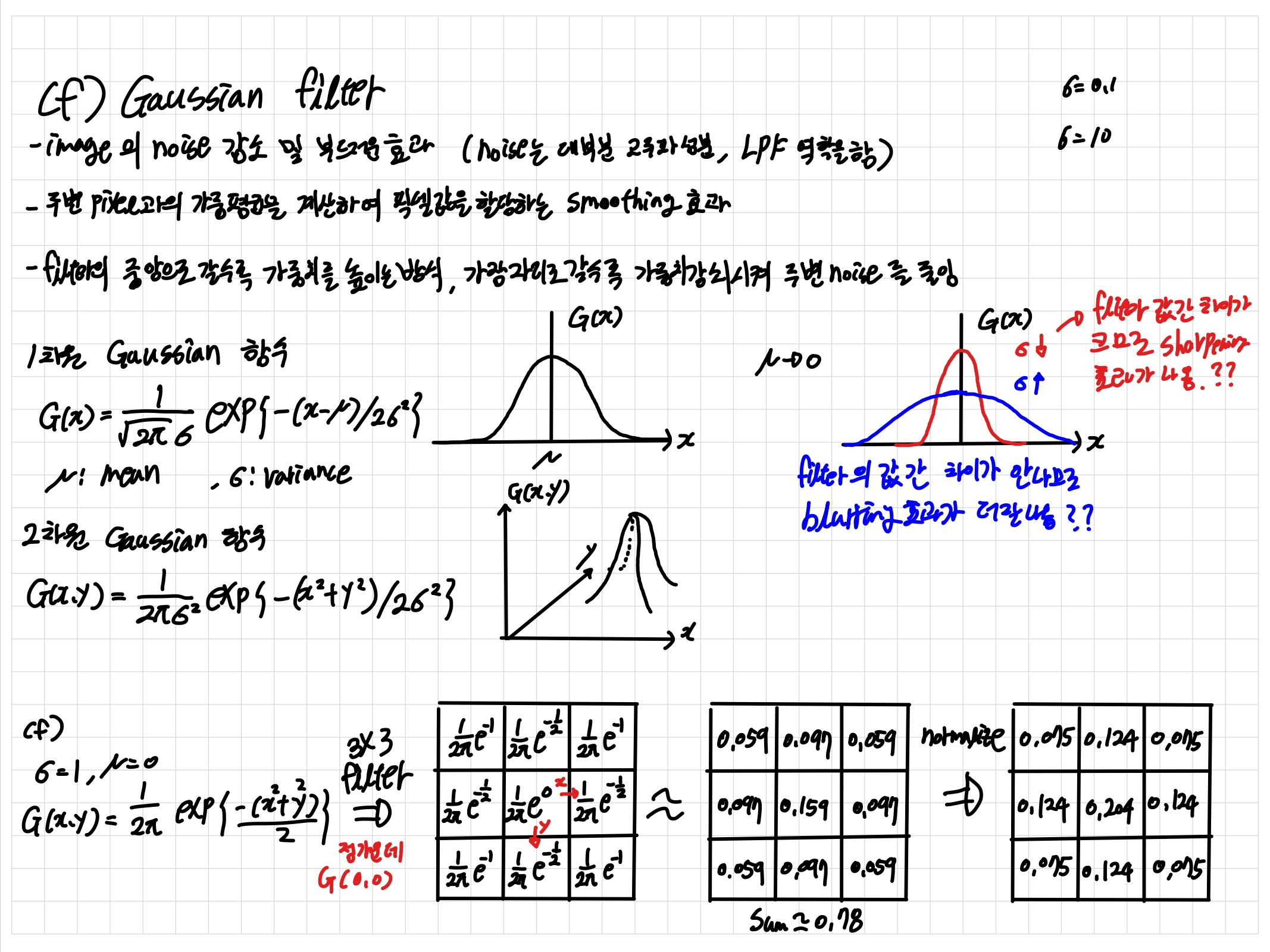
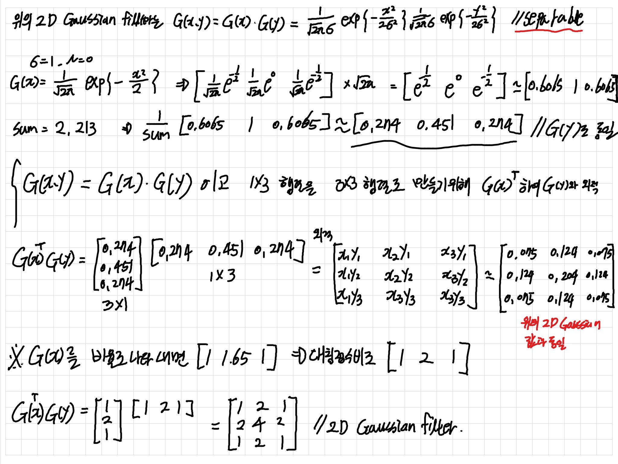
3×3 convolution 연산을 위해 2개의 [imagewidth-1:0] line buffer와 shift register를 이용하여 sliding window 구조를 구현하였습니다.
4-3 Sobel Convolution
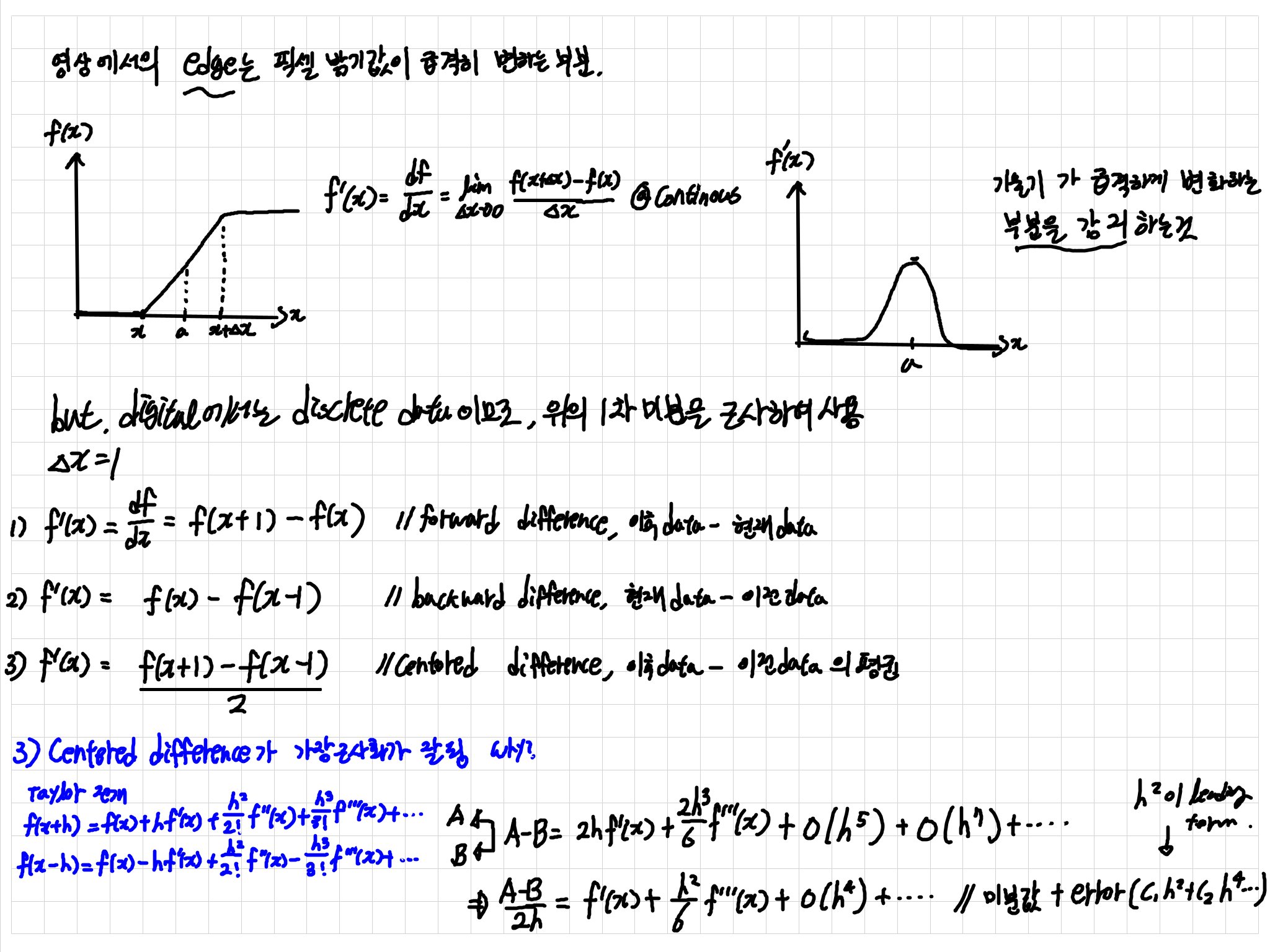
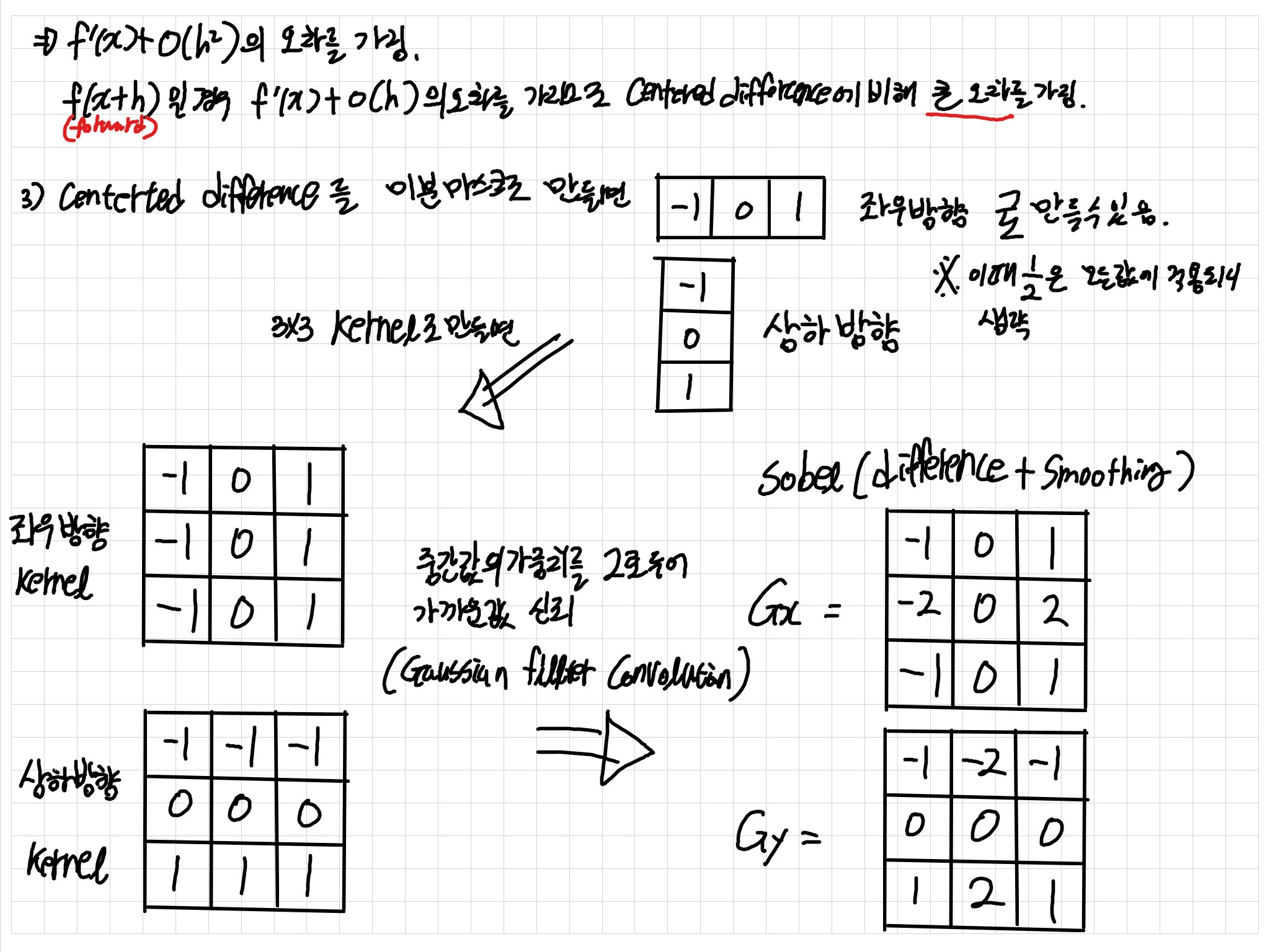
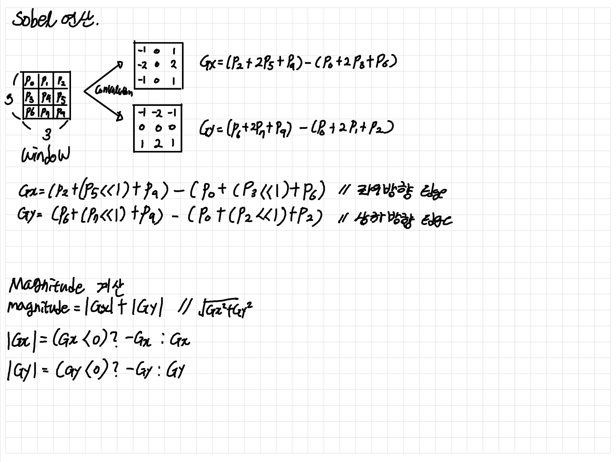
Gx = [[-1,0,1],[-2,0,2],[-1,0,1]]
Gy = [[-1,-2,-1],[0,0,0],[1,2,1]]
mag = |Gx| + |Gy| // sqrt 계산을 절대값으로 근사
5. Latency and Throughput
설계한 Sobel IP는 1 cycle에 1 pixel을 처리하는 pipeline 구조로 구현하였다.
이론적 Throughput
1 pixel / cycle
이론적 Frame 처리 사이클
640 × 480 = 307,200 cycles
이론적 Processing Time
100 MHz 동작 기준
307200 / 100 MHz
≈ 3.07 ms / frame
6. Implementation Issue
초기 설계에서는 여러 픽셀을 동시에 처리하는 병렬 구조를 시도하였습니다. 그러나 sliding window와 Sobel 연산 로직이 병렬로 확장되면서
- 조합 논리 규모 증가
- LUT 사용량 급증
문제가 발생하여 FPGA 자원 사용량이 디바이스 자원을 초과하하여 구조를 단순화하여
1 cycle - 1 pixel pipeline 구조로 수정하였습니다.
7. Test Image & Result
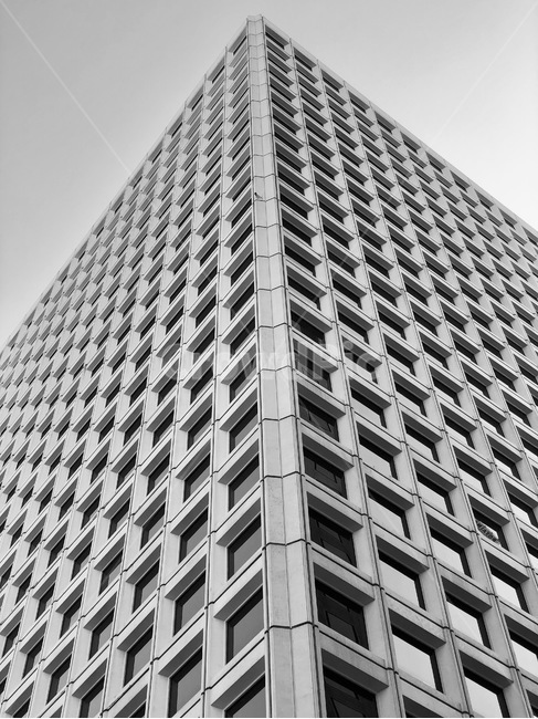
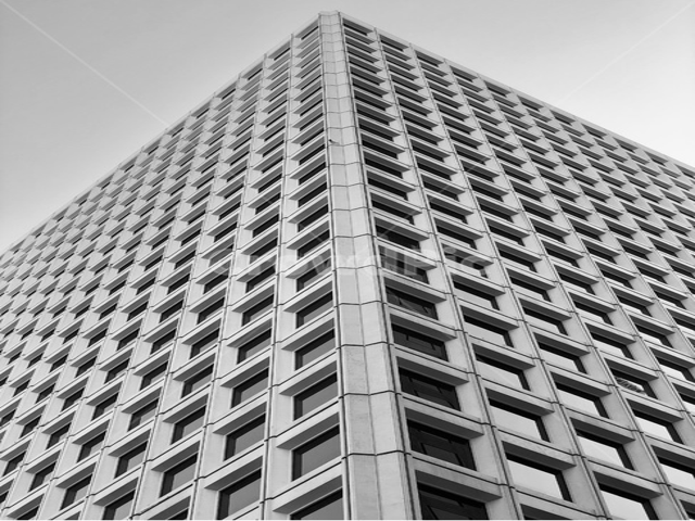
입력 이미지는 python을 통해 grayscale로 변환한 뒤
640 × 480 해상도로 리사이즈하여 DDR에 저장하였습니다.
Input Image Resize
| Original Image | Resized Input(640x480) |
|---|---|
 |  |
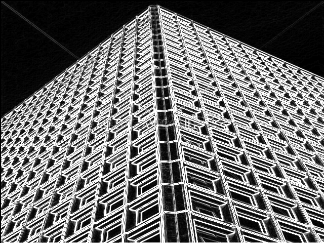
Resized Image를 Python 및 FPGA에서 돌려본결과
Python Reference vs FPGA Output
| Python Reference | FPGA Output |
|---|---|
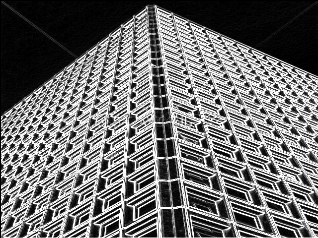 |  |
Difference Check
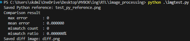
max error : 0
mismatch count : 0
mismatch ratio : 0%
Python 기반 reference 결과와 FPGA 출력 이미지를 비교한 결과 RTL 기반 Sobel IP의 출력이 Python reference 결과와 일치함을 확인하였습니다.
8. Implementation Results
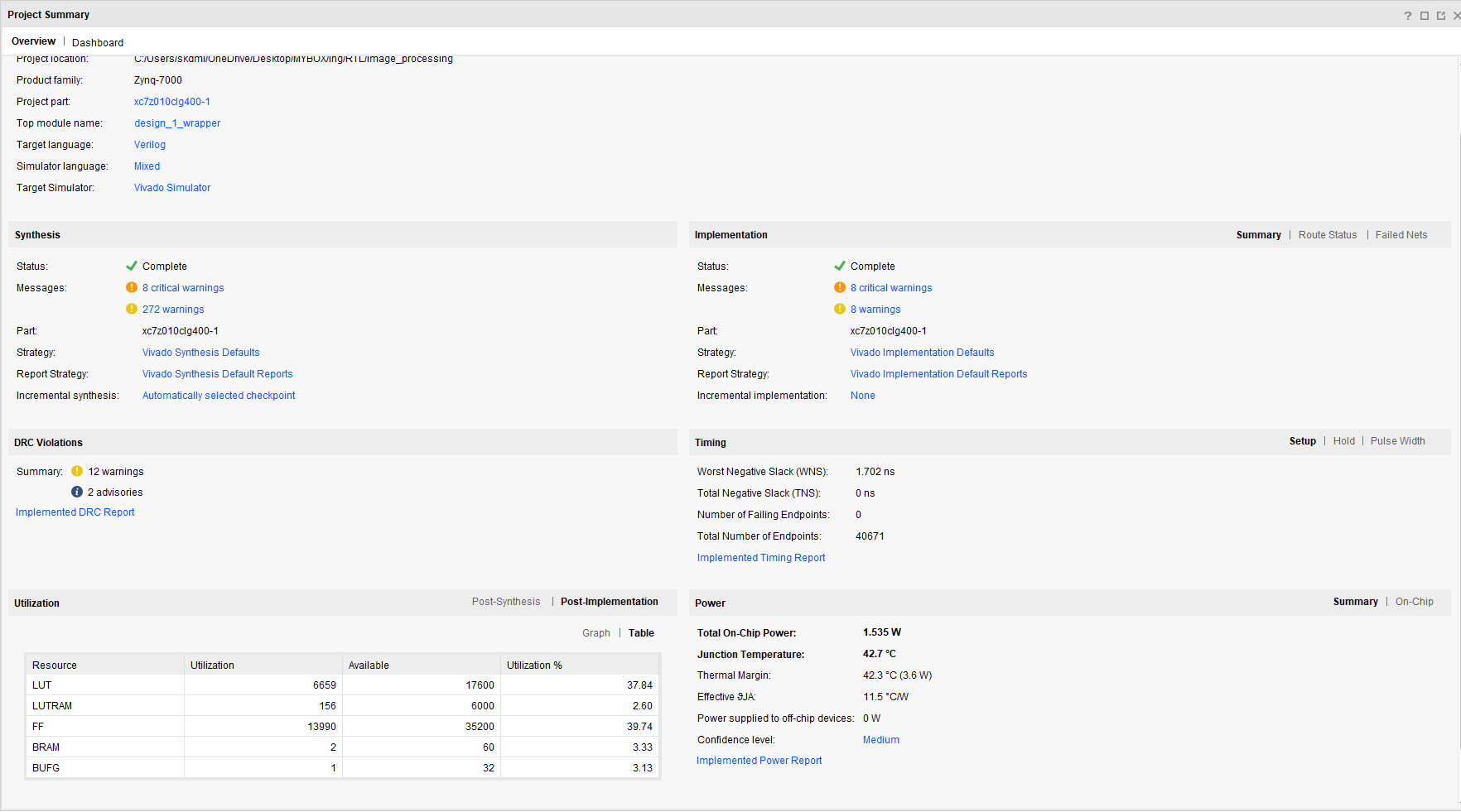
Vivado synthesis 및 implementation 결과
- timing violation 없음
- 설계 정상 구현
주요 결과
| Item | Value |
|---|---|
| WNS | 1.702 ns |
| TNS | 0 ns |
| LUT | 6659 / 17600 (37.84%) |
| FF | 13990 / 35200 (39.74%) |
| BRAM | 2 / 60 (3.33%) |
| On-Chip Power | 1.535 W |
9. Summary
| Item | Value |
|---|---|
| Resolution | 640 × 480 |
| Pixel per cycle | 1 |
| Throughput | 1 pixel / cycle |
| Frame cycles | 307,200 |
| Clock | 100 MHz |
| Processing time(이론적) | 3.07 ms / frame |
결론
해당 시스템을 통해 다음 사항을 확인하였습니다.
- AXI4-Stream 기반 이미지 처리 파이프라인 구현
- DMA 기반 PS-PL 데이터 전송 구조 설계
- Line buffer 기반 sliding window 구조 구현
- Python reference와 RTL 결과의 기능 검증
이를 통해 FPGA 기반 실시간 이미지 처리 시스템의 기본 구조를 구현하고 검증하였습니다.