Chapter 5: Large and Fast: Exploiting Memory Hierarchy
Memory Hierarchy
Disk-memory-cache
Principle of Locality
Temporal locality:
• Items accessed recently are likely to be accessed again soon.
• e.g., instructions in a loop, induction variables.
Spatial locality:
• Items near those accessed recently are likely to be accessed soon.
• E.g., sequential instruction access, array data.
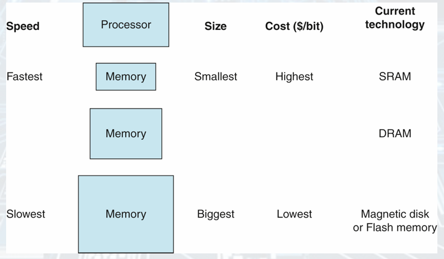
The Basic Structure of a Memory Hierarchy
As the distance from the CPU increases, the size of memories and the access time both increase.
The faster, more expensive memory is close to the processor.
Illusion of memory doing largeest, fastest part
Memory Hierarchy Organization
• A level closer to the processor is a subset of any level further away, and all the data is stored at the lowest level.
• Data is copied between only two adjacent levels at a time.
Terminologies
• Block: the minimum unit of information.
• Hit: if the data requested is found in the upper level.
• Miss: if the data is not found.
• Hit Rate (Hit Ratio): the fraction of memory accesses found in the upper level.
• Miss Rate: (1 Hit Rate).
• Hit time: time to access the upper level of the memory hierarchy.
• Miss penalty: time to replace a block in the upper level with the corresponding block from the lower level + the time to deliver this block to the processor.; replace upper with lower block + deliver block to processor
DRAM Technology
• A single transistor is used to access the charge.
• Must periodically be refreshed.
Read the contents and write back.
Performed on a DRAM “row”.
- Flash Storage: Nonvolatile semiconductor storage
- DIsk Storage: Nonvolatile, rotating magnetic storage.
- Cache Memory: caches take advantage of locality of access, closest to the CPU
Direct Mapped Cache
• Location determined by address.
• Direct mapped: only one choice.
(Block address) modulo (#Blocks in cache)
- Address Subdivision
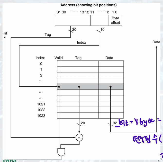
1 word = 4 byte = 32 bit
연속된 수 (0-3, 4-7, 8-11,...)(byte address) 4개씩 항상 같이 움직임
index로 표현 0 1 2 3 ... = word address, 마지막 2bit 버림
ELements and Cache Size
-
Tags: upper portion of address required to identify word, not used to index
-
Valid bit: Indicates whether an entry contains a valid address.
cache index: select the block
Index, tag specifies word in cache block -
block size 2, 2개 word blocks require
tag = 32 - (n + m + 2) bits. -
The number of bits in such a cache is:
index 2bit, valid 1 bit
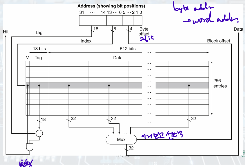
Larger block size
ex) 64 blocks, 16 bytes/block.
• To what block number does address 1200 map?
Block address = floor(1200/16) = 75.
Block number = 75 modulo 64 = 11.
tag 22bits/ index 6 bits (2 entry)/ offset 4 bits (2 byte data)
Large Blocks
Larger blocks exploit spatial locality to lower miss rates.
The miss penalty increases,
• Miss penalty = time required to fetch a block from the memory + time required to load it into the cache.
• Time to fetch a block = latency to the first word + transfer time for the rest of the block.
- The number of blocks is too small or many makes higher miss rate
Handling Cache Misses
• Stall the entire pipeline & fetch the requested word.
• Steps to handle an instruction cache miss:
1. Send the original PC value (PC-4) to the memory.
2. Instruct main memory to perform a read and wait for the memory to complete its access.
3. Write the cache entry, putting the data from memory in the data portion of the entry, writing the upper bits of the address (from the ALU) into the tag field, and turning the valid bit on.
4. Restart the instruction execution at the first step, which will refresh the instruction, this time finding it in the cache.
= org(PC-4) to memory, read it, write it in cache(tag,valid), restart instruction and use cache
+) IF instruction cache/ MEM data cache
Handling Write
store
- Write-through:
Always write the data into both the memory and the cache.
With write buffer: stores the data in the write buffer while waiting to be written to memory.
tag 다르면 바로 cache, main memory에 적음
- Write-back:
Updates values only to the cache, then writes it to the lower level when the block is replaced.
main memory에서 cache로 write back
(final review에 없음)
Example: Intrinsity FastMATH
• Embedded MIPS processor; real system(우린 5개로 배움)
12-stage pipeline.
Instruction and data access on each cycle.
• Split cache: separate I-cache and D-cache,
Each 16KB: 256 blocks × 16 words/block.
D-cache: write-through or write-back.
• SPEC2000 miss rates:
I-cache: 0.4%
D-cache: 11.4%
Weighted average: 3.2%
Designing the Memory to Support Caches
- Main Memory: use DRAMs
- Example
• Example cache block read.
1 bus cycle for address transfer.
15 bus cycles per DRAM access.
1 bus cycle per data transfer.
• For 4-word block, 1-word-wide DRAM.
Miss penalty = 1 + 4×15 + 4×1 = 65 bus cycles.
Bandwidth = 16 bytes / 65 cycles = 0.25 B/cycle.
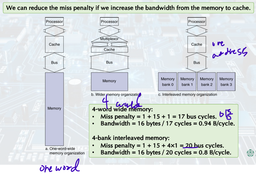
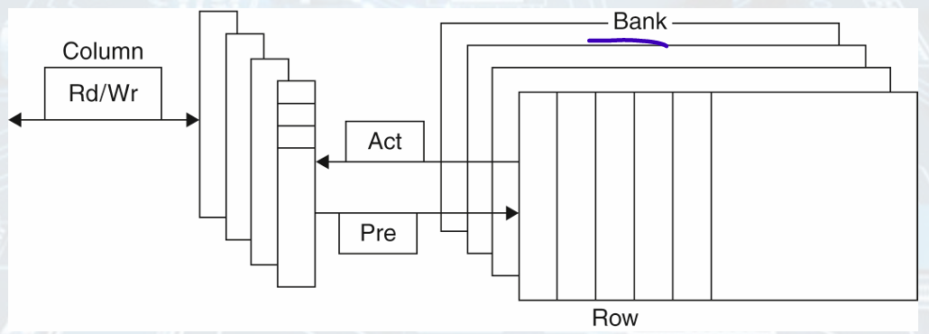
Memory Interleavingp30
The memory chips are organized in banks to read or write multiple words in one access time.
Cache Performance
- improving cache performance:
Reducing the miss rate by reducing the probability that two different memory blocks will contend for the same cache location.
Reducing the miss penalty by adding an additional level to the hierarchy. Multilevel caching.
- With increased Clock rate:
Relative cache penalties increase
If a machine improves both clock rate and CPI, it suffers a double hit.
The lower the CPI, the more pronounced the impact of stall cycles. (stall cycles 중요)
If the main memories of two machines have the same absolute access times, a higher CPU clock rate leads to a larger miss penalty.
Formula
CPU time = (CPU execution clock cycle + Memory-stall clock cycles) x Clock cycle time
+)
Performance = 1 / Execution time
CPI = Clock Cycles / Instruction Count (Clock Cycles per Instruction)
Execution time Clock Cycles, if same clock cycle time
Execution time CPI, if same clock cycle time and Instruction count
- Memory-stall clock cycles
- 과정: 넘어가기
Memory-stall clock cycles = Read-stall clock cycles + Write-stall cycles
Real-stall clock cycles = x Read Miss Rate x Read Miss Penalty
Write-stall cycles(for write-through) = ( x Write Miss Rate x Wirte Miss Penalty) + (Write Buffer Stall)
In most write-through cache organization,
read = write miss penalty (time to fetch the block from memory)
ignore (Write Buffer Stall)
Example Cache Performance
Q) Instruction cache miss rate: 2%, Data cache miss rate: 4%.
CPI: 2 without any memory stalls. Miss penalty: 100 cycles for all misses.
• How much faster a machine would run with a perfect cache that never missed?
Frequency of all loads and stores: 36%. Calculate CPIs and compare them.
Sol)
-Instruction miss cycles = I x 2% x 100 = 2.00 x I (I x miss rate x miss penalty)
-Data miss cycles = I x 36% x 4% x 100 = 1.44 x I (load,store 36% x I ;memory accesses/program)
-Total number of memory-stall cycles = 3.44 x I (sum of two)
-Total CPI = 2(without memory stall) + 3.44 x I/I(memory stall) = 2 + 3.44 = 5.44 (CPI = Clock Cycles / Instruction Count)
-The performance with perfect cache is better by 2.72
Performance = 1/Execution Time, Execution Time CPI
perfect Performance / this performance = this CPI / perfect CPI(without memory stall) = 5.44 / 2 = 2.72
Associative Cache
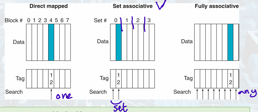
- Direct mapped cache:
A memory block can go in exactly one place in the cache. - Fully associative cache:
A memory block can be placed in any location in the cache.
All entries must be searched. - Set associative cache:
The middle range of design between direct mapped and fully associative.
There are a fixed number of locations(N-way) where each block can be placed.
Position of a Memory Block
A direct-mapped cache: (Block number) modulo (Number of cache blocks)
A set-associative cache: (Block number) modulo (Number of sets in the cache)
- Tag Searching
Set-Associative: All the tags of all the elements of the set must be searched.
Fully-Associative: All tags of all the blocks in the cache must be searched.
Variations of Set Associative
Increasing the associativity decreases the number of sets, while increasing the number of elements per set.
It decreases the miss rate while increases the hit time.
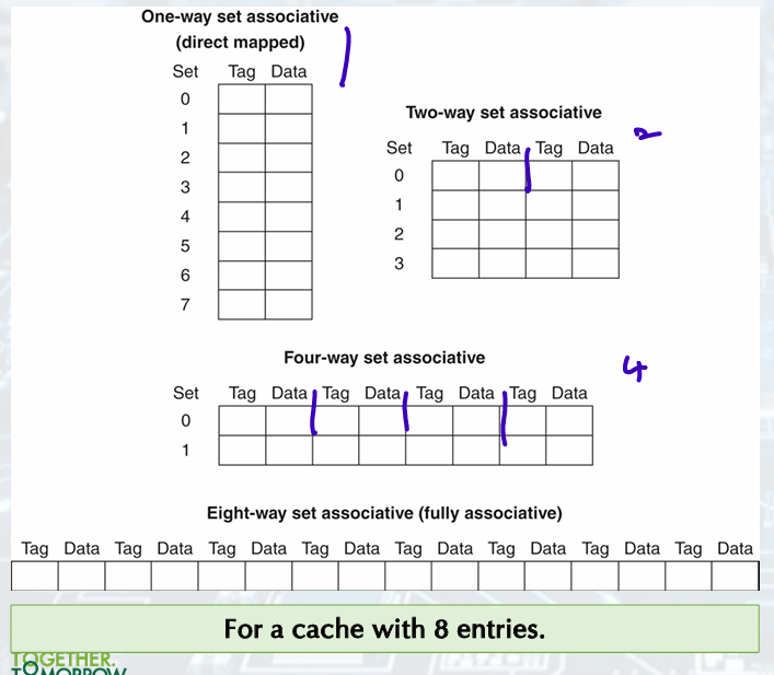
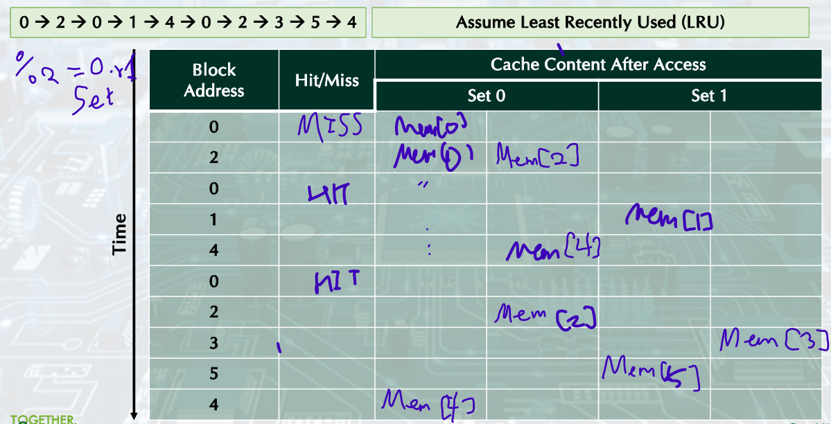
Example: Misses and Associativity in Cache
2-Way Set-Associative Cache

최근에 쓰이지 않은 것 replace
- Address for Set Associative
tag, index, block offset; the address of the desired data within the block. - 4-Way Set Associative Cache
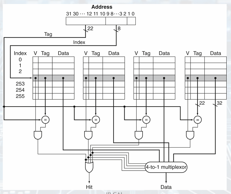
Block Replacement Policy: Least-Recently Used (LRU)
The block replaced is the one that been unused for the longest time.
It is implemented by keeping track of when each element was used.
-
Temporal locality, effective/ With 4-way or greater, requires complicated hardware and much time to keep track of this.
high associativity, same as random replacement policy -
Example Block Replacement
Multilevel Caches
Primary cache: small, fast, focus on minimal hit time
Level-2 cache service: larger, slower, faster than main memory, focus on a low miss rate to avoid main memory access
- Example:
Q) A base CPI of 1.0 with a perfect cache.
A clock rate of 4GHz.
Main memory access time of 100 ns.
Miss rate per instruction at the primary cache is 2%.
• How much faster will the processor be if we add a secondary cache that has a 5 ns access time?
It is large enough to reduce the miss rate to main memory to 0.5%.
Sol)
Miss penalty = access time x clock rate (1 / clock cycle time)
1/GHz = ns 단위 맞음
-With just primary cache:
Miss penalty =
Effective CPI = Perfect cache CPI + memory stall CPI(miss rate x miss penalty) = 1 + 0.02 x 400 = 1 + 8 = 9
-With L1 and L2 cache:
Miss penalty to L2 cache =
Effective CPI = Perfect cache CPI + L1 to L2 stall CPI(L1 miss rate x miss penalty to L2) + L2 to main memory stall CPI(L2 miss rate to main memory x miss penalty to main memory) = 1 + 0.02 x 20 + 0.005 x 400 = 1 + 0.4 + 2 = 3.4
-Performance ratio: L2Performance / L1Performance = L1 CPI / L2 CPI = 9 / 3.4 = 2.6
(다른 수업)
Virtual Memory
• Use main memory as a “cache” for secondary (disk) storage; Managed jointly by CPU hardware and the operating system (OS).
• Programs share main memory.
Each gets a private virtual address space holding its frequently used code and data.
Protected from other programs.
• CPU and OS translate virtual addresses to physical addresses.
VM “block” is called a page.
VM translation “miss” is called a page fault.