Contents
1. Symbols you must know
2. What a MOSFET is made of
3. The one big idea: it is a capacitor
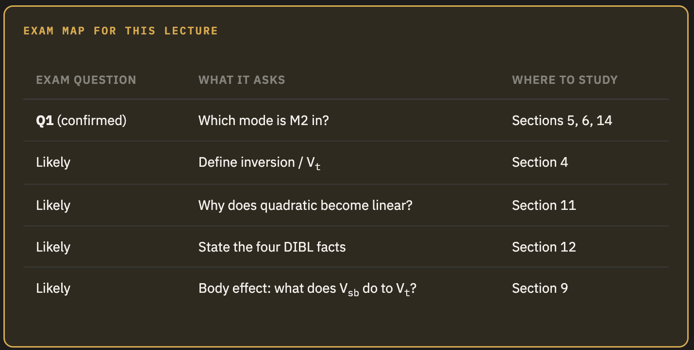
4. How a channel appears
5. The three operating modes ★
6. Finding the source ★
7. The current equations
8. A fully worked number example
9. Threshold voltage in detail
10. Why scaling broke the model
11. Velocity saturation ★
12. DIBL ★
13. PMOS and new structures
14. Exam Q1, fully solved ★
Symbols you must know
Before anything else, here is every symbol used in this lecture. If a formula later looks scary, come back here. Most of the difficulty in this course is just unfamiliar notation.
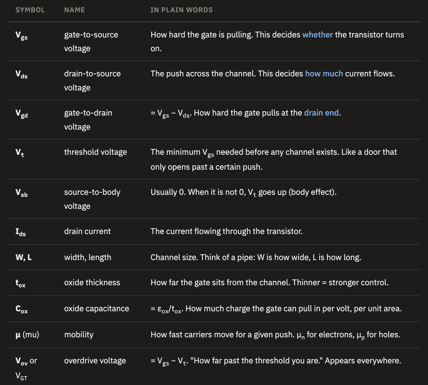
Vgs decides IF the transistor is on. Vds decides HOW it behaves once it is on.
Every mode question on the exam is answered by checking those two things in that order.
What a MOSFET is made of
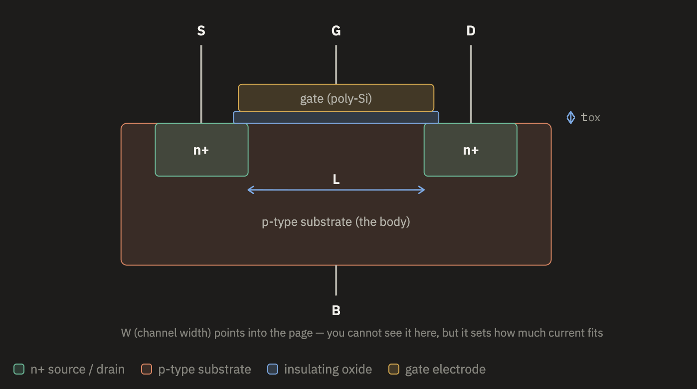
MOSFET stands for Metal–Oxide–Semiconductor Field Effect Transistor. The name is literally a list of the three layers, stacked from top to bottom:
- Metal — the gate electrode on top. (Modern chips use polysilicon, but the name stuck.)
2.Oxide — a very thin insulating layer of SiO₂ underneath the gate. - Semiconductor — the silicon substrate at the bottom.
Then two heavily doped regions are implanted into the substrate on either side. In an NMOS these are n+ regions sitting in a p-type substrate.
There are four terminals, not three
Everyone remembers Gate, Source and Drain. The fourth is the Body (also called bulk or substrate). It is usually left out of schematics because it is always tied to the same place: ground for NMOS, VDD for PMOS. But it exists, and Section 9 shows when it bites you.
The three dimensions
Why this matters later
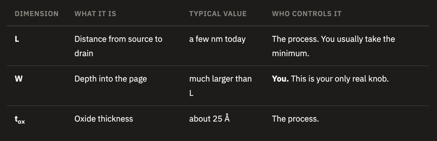
Since L and tox are fixed by the factory, every "size this transistor" problem is really a "pick W" problem. When Lecture 4 asks you to write 2W or 4W next to a transistor, this is what it means.
The one big idea: it is a capacitor
Here is the single sentence that explains how a transistor works:
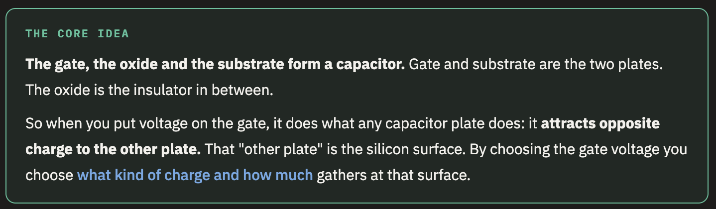
Two consequences follow immediately, and both matter:
1. The gate draws no DC current
The oxide is an insulator, so nothing flows through it. In steady state the gate current is zero. This is the big advantage over bipolar transistors, which need base current continuously. It is also why CMOS logic burns no power while sitting still.
2. Thinner oxide means stronger control
Gate capacitance per unit area
Cox = εox / tox
Smaller tox gives bigger Cox, which means the gate pulls in more charge per volt. That is why the industry kept making the oxide thinner. Remember this — it comes back in Section 12 as one of the fixes for DIBL.
How a channel appears
Now let's slowly raise the gate voltage on an NMOS and watch what happens at the silicon surface. There are three stages.
Remember the starting point: the substrate is p-type, which means it is full of holes (positive carriers) and has very few electrons.
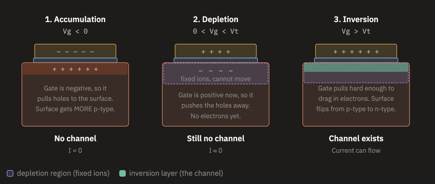
Stage by stage
Stage 1 — Accumulation (Vg negative). A negative plate attracts positive charge. The substrate's holes are positive, so they crowd up to the surface. The surface becomes even more p-type. Now look at what you have from source to drain: n+ / p / n+. That is two diodes pointing at each other. Whichever direction you push, one of them is reverse-biased and blocks. No current.
Stage 2 — Depletion (Vg positive but small). A positive plate repels positive charge, so the holes get pushed down into the substrate. They leave behind the doping atoms they came from, which are negatively charged and bolted into the crystal — they cannot move, so they cannot carry current. The surface now has no free carriers at all. It is "depleted". Still no current.
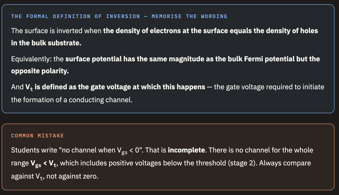
Stage 3 — Inversion (Vg > Vt). Push the gate harder and it starts dragging in electrons — the minority carriers, the rare ones. They pile up in a thin sheet right at the surface. That sheet is n-type. Now the path reads n+ / n / n+, all the same type, one continuous wire. Current can flow.
The three operating modes ★
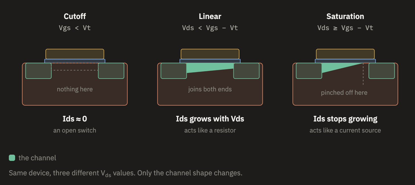
Once a channel exists, applying Vds makes current flow. How much depends on the shape of the channel, and there are three cases.
First, the one rule that explains everything

Let's apply it. Call the voltage inside the channel at some position V(y).
- At the source end, the channel voltage is 0 (it is connected to the source). So gate-to-channel = Vgs − 0 = Vgs. This is the largest it gets.
- At the drain end, the channel voltage is Vds. So gate-to-channel = . This is the smallest it gets.
That is why the channel is thick at the source and thin at the drain. The gate has less pull where the channel voltage has already risen.
Put numbers on it
Take Vgs = 2 V, Vt = 0.5 V, and try three values of Vds:
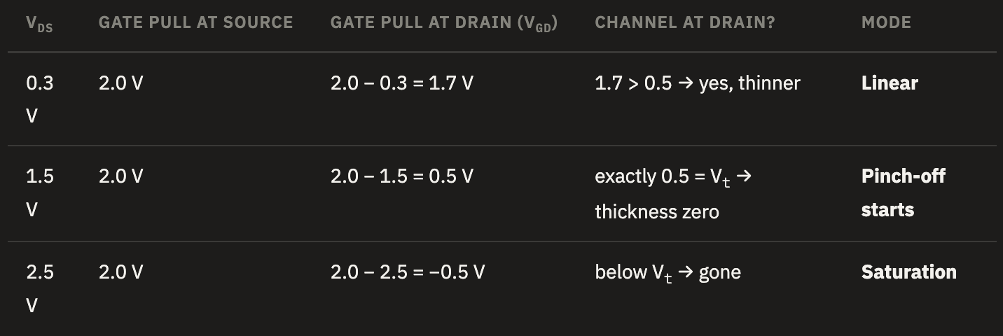
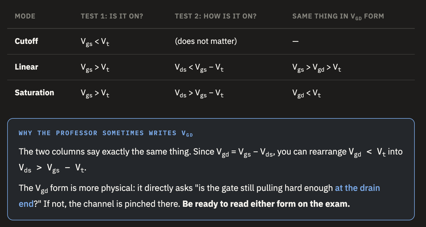
Notice where the boundary landed: Vds = 1.5 V = Vgs − Vt. That is not a coincidence — it is the definition.
The saturation boundary (memorise this)
Vds,sat = Vgs − Vt also written Vov or VGT
Why current does not stop at pinch-off
This confuses almost everyone. If the channel is cut, why is there still current?
-
The channel is not cut, it is just empty of inversion charge. That small region becomes a depletion region, not an insulator.
-
A huge electric field appears across that little gap. The channel always holds Vds,sat across it. Everything above that — the amount (Vds − Vds,sat) — drops across the narrow pinched-off region. Small distance, big voltage, enormous field.
-
So electrons are swept across instantly. Any electron that reaches the pinch-off point gets yanked to the drain.
-
The channel, not the gap, sets the current. And the voltage across the channel is frozen at Vds,sat no matter how high you push Vds. So the current stops growing. That is saturation.
Picture it
Water flows through a pipe and then falls off a cliff into a pool. Making the cliff taller does not make more water come out of the pipe. The pipe sets the flow rate; the drop does not. The pipe is the channel and the cliff is Vds beyond saturation.
Finding the source ★
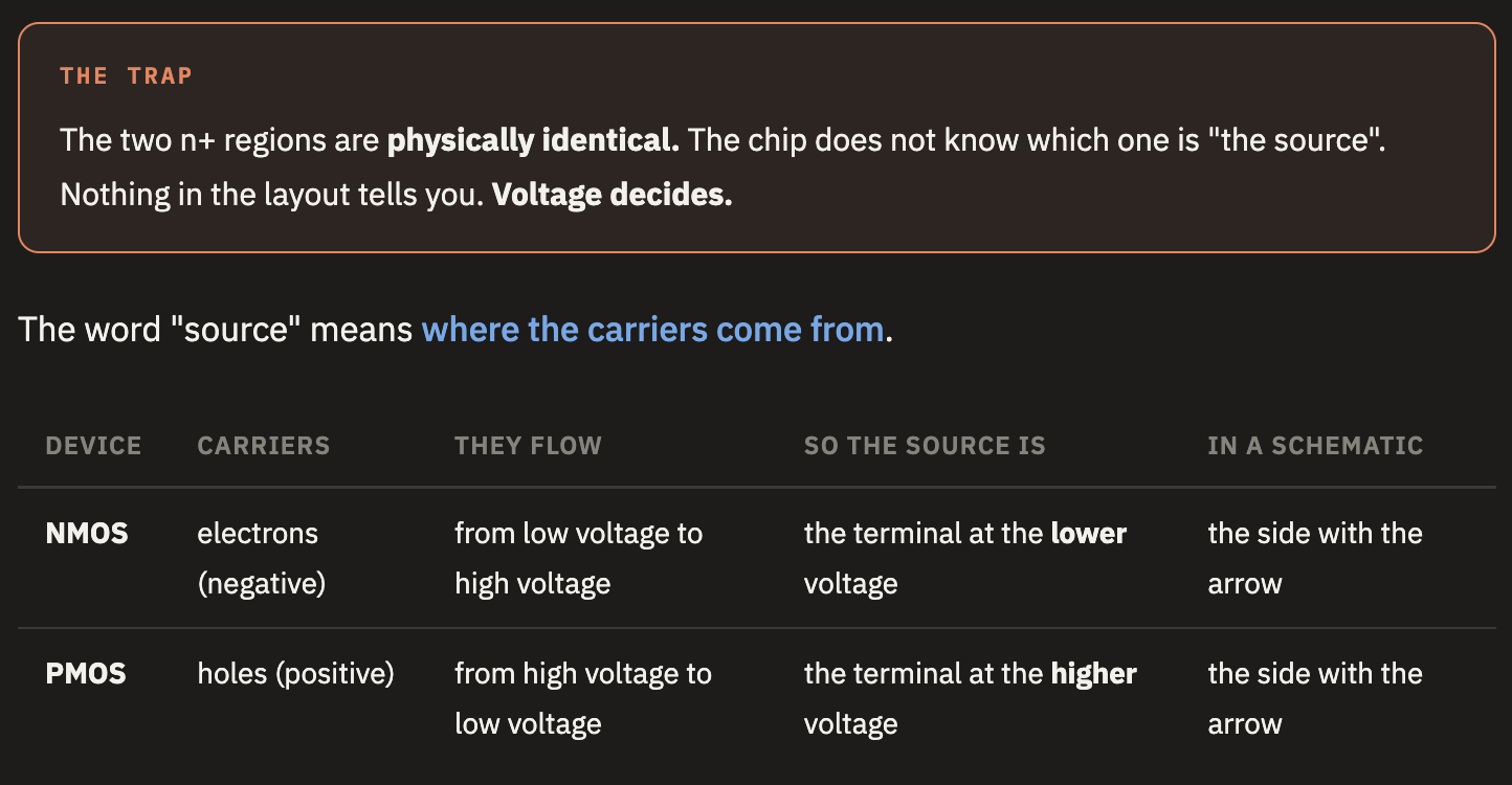
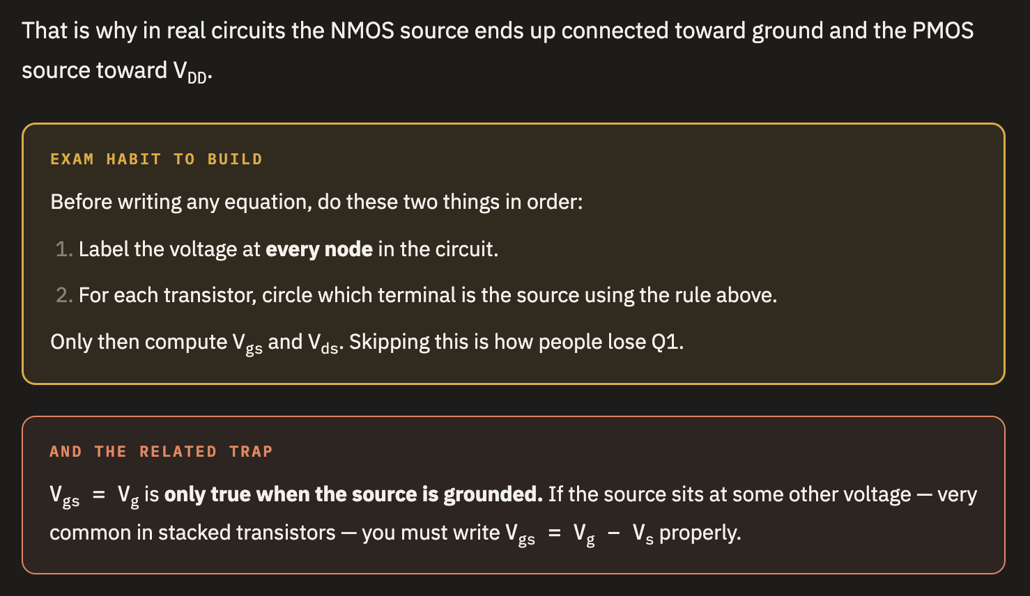
This is the step most people get wrong on the exam, and it comes before every mode calculation
A fully worked number example
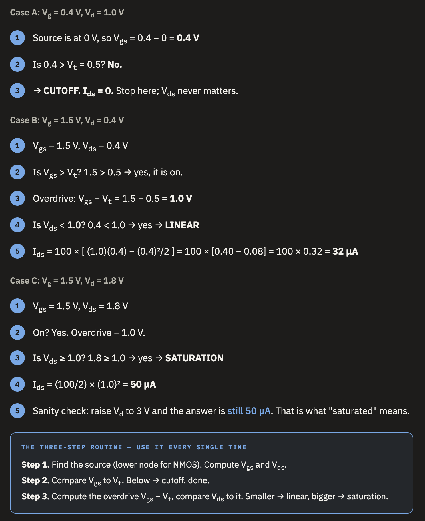
Work through this with a pencil. It is exactly the shape of an exam calculation.
Given
An NMOS with Vt = 0.5 V. Take μnCox(W/L) = 100 μA/V² to keep the arithmetic clean. The source is grounded.
Velocity saturation ★
DIBL ★
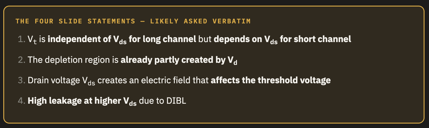
DIBL = Drain-Induced Barrier Lowering. The name tells you the whole story once you know what the "barrier" is.
What is the barrier?
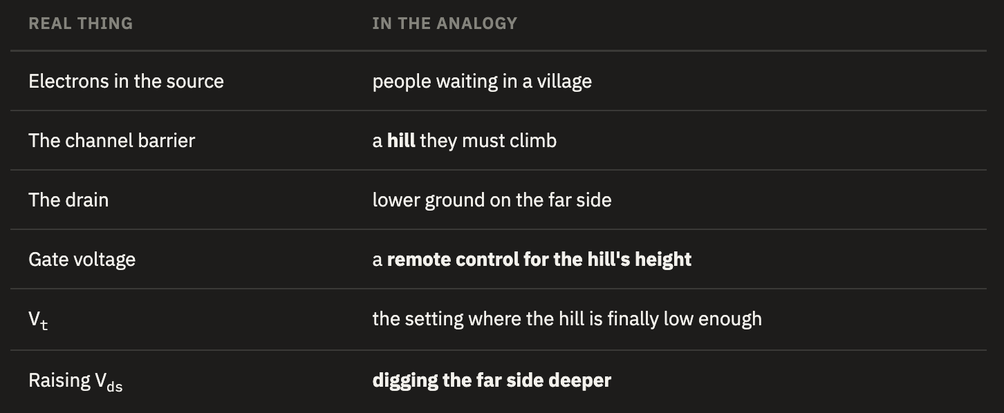
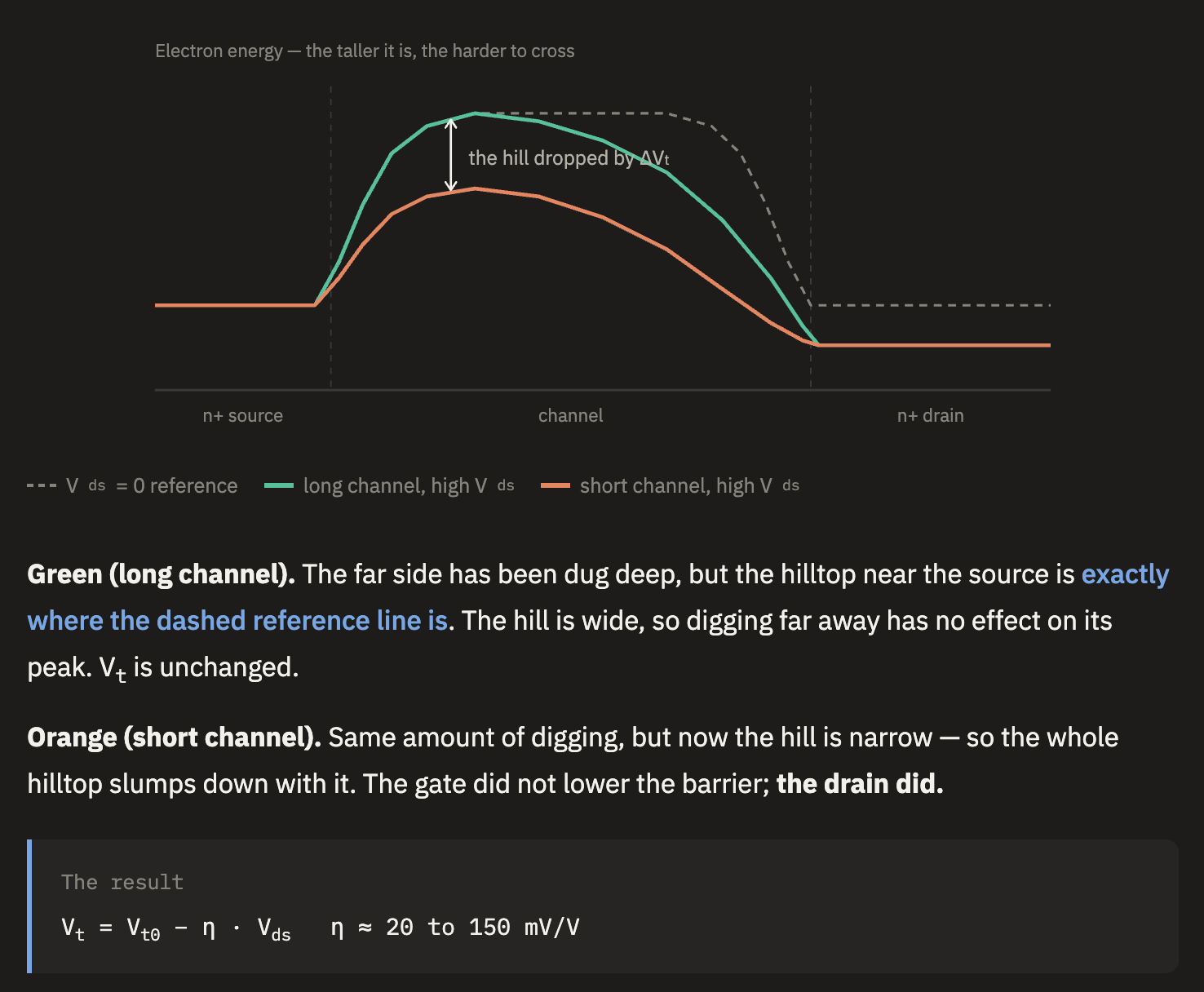
For an electron to leave the source and enter the channel, it must climb over an energy hill. Turning the transistor on means lowering that hill until electrons can get across.
Map the pieces
Why this is so damaging
The killer detail
When is Vds largest? When the transistor is OFF — because then the full VDD sits across it.
So DIBL is strongest exactly when you want the device shut tight. The threshold is lowest at the worst possible moment. That is the meaning of "high leakage at higher Vds".
And leakage depends exponentially on Vt, so a 100 mV drop can multiply leakage by roughly twenty. Multiply by billions of transistors and that is your battery.
Exam Q1, fully solved ★
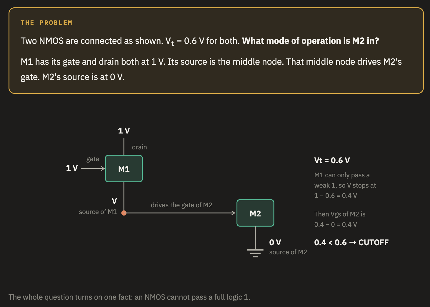
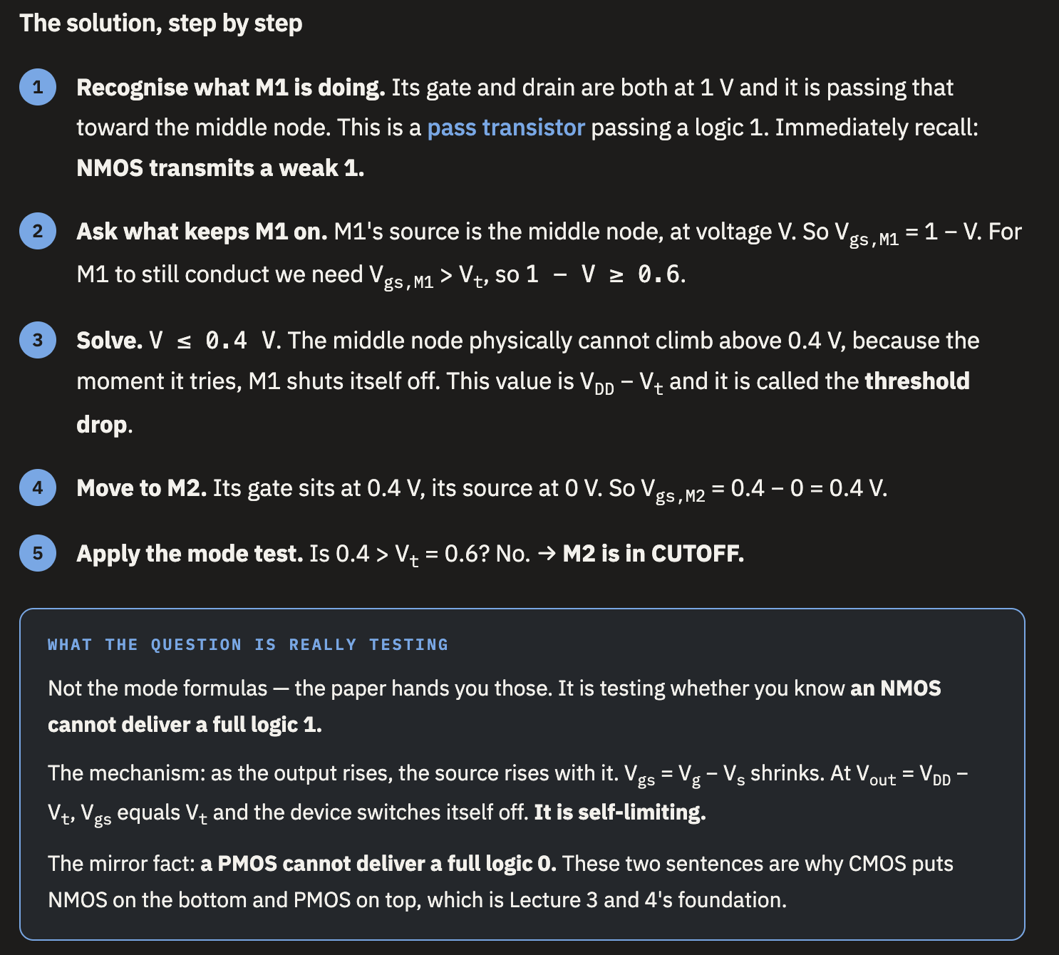
Traps to avoid on this question
- Assuming M2's gate is at 1 V. Read the circuit carefully — trace what actually connects to each gate.
- Forgetting to find the middle node voltage first. You cannot evaluate M2 until you know V.
- Getting the source backwards. For M1, the 1 V terminal is the drain (higher) and the middle node is the source (lower).
- Ignoring body effect. M1's source is above ground, so its real Vt is higher than 0.6 V, making V even lower than 0.4 V. The conclusion is unchanged, but writing one line about this shows mastery.