VLSI Design
1.spice
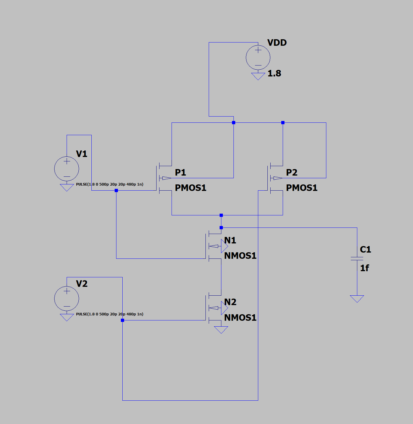
CMOS NAND GATEMosfet SizeEdit -> spice directivePulsectrl + right click waveform titleyou can check avg.power
2.2. The MOS Device
Before anything else, here is every symbol used in this lecture. If a formula later looks scary, come back here. Most of the difficulty in this course
3.Lec2. MOSFET
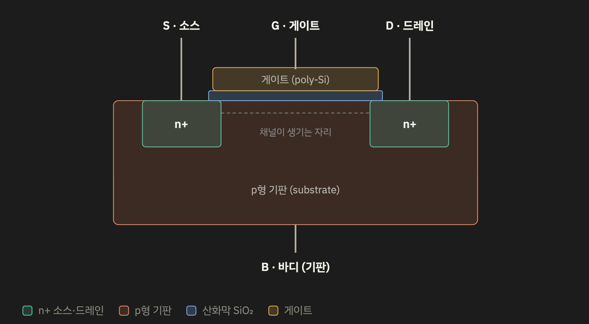
MOSFET은 이름 그대로 Metal–Oxide–Semiconductor Field Effect Transistor입니다. 게이트가 산화막을 사이에 두고 반도체 위에 얹혀 있는 구조죠.꼭 챙겨야 할 두 가지단자는 4개입니다. G, S, D 말고 바디(B)가 있어요. 수
4.Lec3. CMOS Inverter
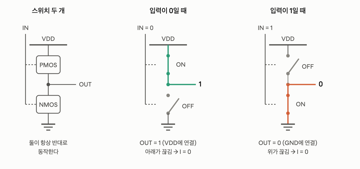
앞서 배운 걸 떠올려 보세요. 디지털에서 트랜지스터는 두 상태만 씁니다. 완전히 켜짐 이거나 완전히 꺼짐(차단,$I≈0$). 그 중간은 지나가기만 하죠. 그래서 그냥 스위치로 취급해도 됩니다.핵심은 상보적(complementary) 이라는 점입니다. 두 스위치가 절대
5.Lec4. Complex gate, Sizing
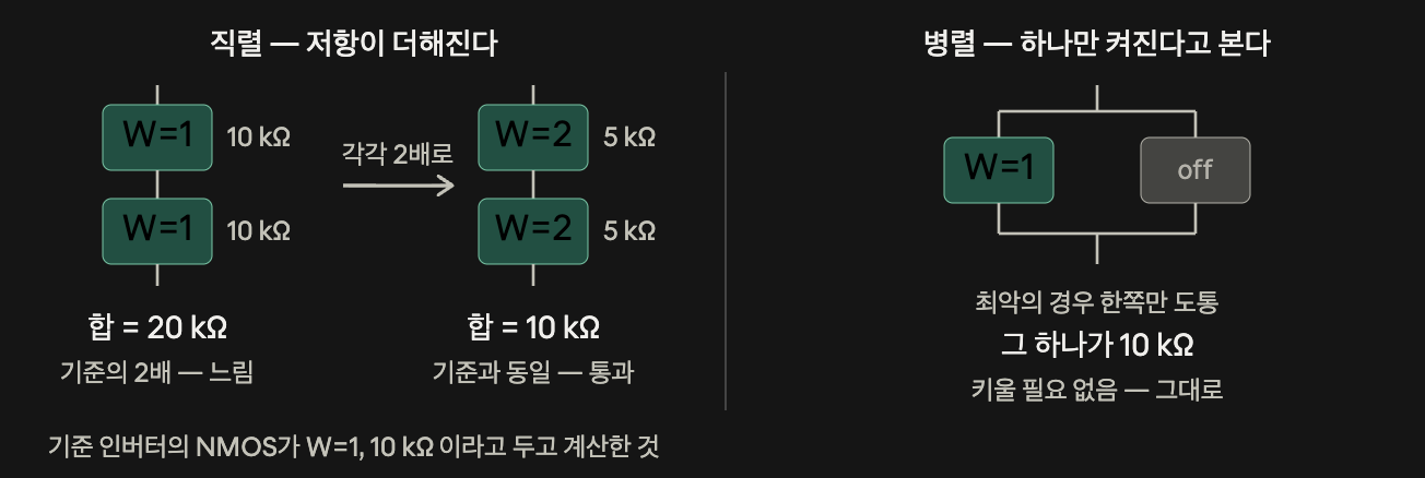
The whole lecture starts from one simplification: represent an "on" transistor as a resistor R. Then a network of transistors becomes a network of res
6.Lec5. Capacitance, LE
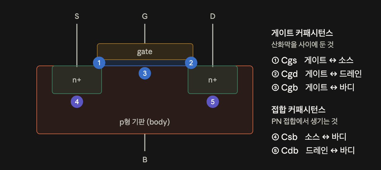
Two formulas you already know both contain C, and nothing else in them is really under your control:tpd ≈ 0.69 · Ron · CL Pdyn = α · CL · V2 · fSo
7.Progressive Sizing
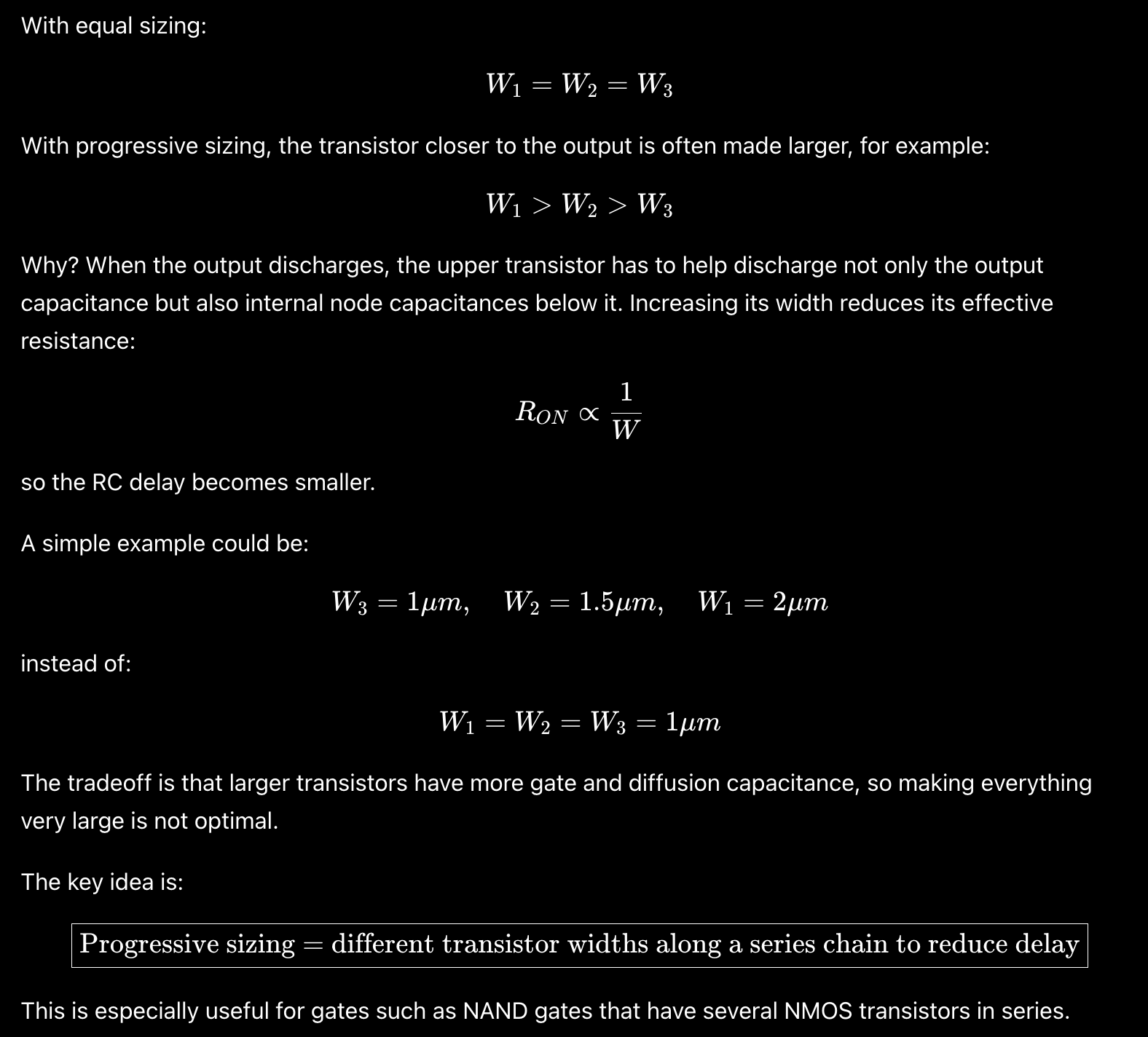
In VLSI, progressive sizing means making transistors in a series stack gradually larger depending on their position, instead of giving every transisto
8.Midterm-1

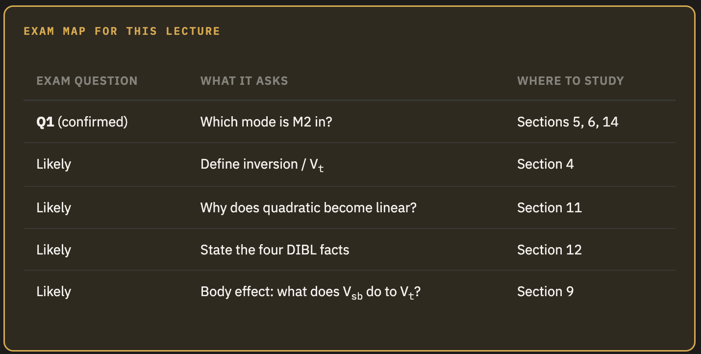
Two NMOS are connected as shown here. What mode of operation (cutoff, linear, saturation) is M2 in? Vt for both MOS is 0.6V. Useful info: The side wit
9.VLSI Power
VLSI PowerVdd -> Capacitor -> GndDynamic powercapacitance swithcingcrowbar currentStatic powerLeakage currentrelation with energy and delayLow swing c