the ARM Cortex-M3 Processor - 4
Chapter 5 Memory Systems
5.1 MEMORY SYSTEM FEATURES OVERVIEW
First, it has a predefined memory map that specifies which bus interface is to be used when a memory location is accessed. This feature also allows the processor design to optimize the access behavior when different devises are accessed.
Another feature of the memory system is the bit-band support. This provides atomic operations to beit data in memory or peripherals. The bit band operations are supported only in special memory regions. This topic is covered in more detail later in this chapter.
The Cortex-M3 memory system also supports unalighned transfers and exclusive accesses.
5.2 MEMORY MAPS
This makes it easier to port software from one Cortex-M3 to another. For example, Components descried in previous sections, such as Nested Vectored Interrupt Controller(NVIC) and Memory Protection Unit(MPU),have the
4. GPIOA 의 PIN5 제어하기

앞서 언급한 것과 같이 GPIOA의 PIN5를 제어하기 위해서는 GPIO_BSRR 레지스터와 GPIO_BRR 레지스터의 각각 5번 Bit를 제어해야 한다. 각각 레지스터의 5번 Bit는 아래와 같이 Bit band alias 주소를 계산할 수 있다.

GPIOA_PIN_5_SET = 0x42000000 + (0x40010810 - 0x40000000) * 32 + (5 * 4);
GPIOA_PIN_5_RESET = 0x42000000 + (0x40010814 - 0x40000000) * 32 + (5 * 4);
same memory locaitons in all Cortex-M3 products. Nevertheless, the memory map definition allows great flexibility so that manufacturers can differentaibte thir Cortex M3 based product from others.
Some of the memory locations are allocated for private peripherals such as debugging components.
They are located in the private peripheral memory region.
These debugging components include the follwing:
- Fetch Patch and Breakpoint Unit(FPB)
- Data Watchpoint and Trace Unit(DWT)
- Instrumentation Trace Macrocell(ITM)
- Embedded Trace Macrocell(ETM)
- Trace Port Interface Unit(TPIU)
- ROM Table
The Cortex-M3 processor has a total of 4GB of Address space. Program code can be located in the code region, the Program code can be located in the code region, the Static Random Access MEmory (SRAM) region, or the external RAM Region. However, it is best to put the program code in the code region because with this arragement, the instrcution fetches and data accesses are carried out simultaneously on two separeate bus interfaces.
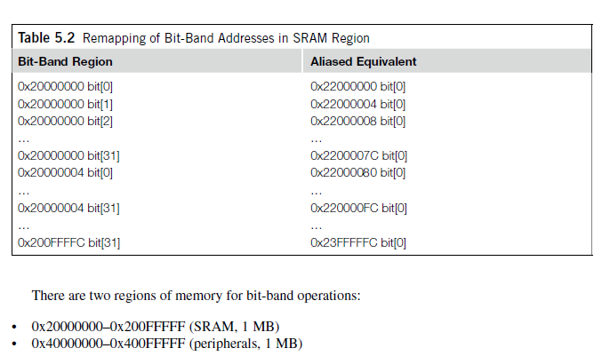
The SRAM memory range is for connecting internal SRAM. Access to this region is carried out via the system interface bus. In this region , a 32-MB ragne is defined as a bit-band alias.Within the 32 bit band alias memory range, each word address represents a single bit in the 1-MB bit band region. A data write access to this bit band alias memory range will be converted to an atomic READ MODIFY WRITE operation to the bit band region so as to allow a program to set or clear individual data bits in the memory. The bit band operation applies only to data accesses not instruction fetches.
By putting Boolean information(single bits) in the bit-band region, we can pack multiple Boolean data in a single word while still allowing them to be accessible individually via bit band alias,
Another 0.5 GB Block of address range is allocated to on-chip peripherals. Similar to the SRAM region, this region supports bit-nand alias and is accessed via the system bus interface. However, instruction execution in his regions is not allowed. The bit and support in the peripheral region makes it easy to access or change control and status bits of peripherals,
Two slots of 1 GB memory space are allocated for external RAM and external devices. The difference between the two is that program execution in the external device region is not allowed, and there are some differences with the caching behaviors.
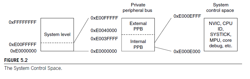
The last 0.5 GB memory is for the system level components, internal peripheral buses, exteranl peripheral bus, and vendor specific system peripherals. There are two segments of the private peripheral bus(PPB):
Advanced High Performance Bus PPB, For Cortex-M3 internal AHB peripherals only ; this includes NVIC,FPB, DWT, and ITM
The NVIC is located in a memory region called the system control space(SCS)
Besides providing interrupt control features, this region also provides the control registers for SYSTICK, MPU, and code debugging control.
5.3 MEMORY ACCESS ATTRIBUTES
The memory map shows what is included in each memory region. Aside from decoding which memory block or device is accessed, the memory map also defines the memory attributes of the access. The memory attributes you can find in the Cortex-M3 processor include the following:
-
Bufferable : Write to memory can be carried out by a write buffer while the provessor continues on next instruction excution.
-
Cacheable : Data obtained from memory read can be copied to a memory caches so that next time it is accessed the value can be obtained from the cache to speed up the progrma excution.
-
Executable : The processor can fetch and execute program code from this memory region.
-
Sharable : Data in this memory region could be shared by multiple bus masters. Memory system needs to ensure coherency of data between different bus masters in shareable memory region.
The Cortex-M3 bus interfaces output the memory access attributes information to the memory system for each instruction and data transfer. The defulat memory attribute settings can be overriden if MPU is present and the MPU region confugurations are programmed differently from the default.
- Code Memory region (0x00000000 - 0x1FFFFFFF) : This region is executable, and the cache attriute is write through(WT). You can put data memory in this region as well. If data operations are carried out for this region, they will take place via the data bus interface. Write transfer to this regions are bufferable.
-SRAM memroy region(0x20000000 - 0x3FFFFFFF ): This region is intenede for on chip RAM. Write Transfers to this region are bufferable, and the cache attribute is write back , wrtie allocated (WB-WA). This region is executable , so you can say copy program code here and execute it.
-
Peripheral region (0x40000000 - 0x5FFFFFFF) : This region is intended for peripherals. The accesses are noncacheable. You cannot execute instruction code in this region(Execute Never, or XN in ARM documentation, such as the Cortex M3 TRM).
-
External RAM region(0x60000000 - 0x7FFFFFFF) : This region intenede for ether on chip or off chip memory. The accesse are cachable(WB-WA), and you can execute code in this region.
-
External devices is intended for external devices and/or shared memory that needs ordering/nonbuffered accesses.
-
System region : This region is for private peripherals and vendor-specific devices. It is non executable.
5.4 DEFAULT MEMORY ACCESS PERMISSIONS
The Cortex-M3 memory map has a default configuration for memory access permissions. This prevents user programs(non-previleged) from accessing system control memory spaces such as the NVIC.
The default memory access permission is used when either no MPU is present or MPU is preset but disabled.
If MPU is present and enabled, the access permission in the MPU setup will determine wheter user accesses are allowed.
Table 5.1 Default Memory Access Permissions
| Memory Region | Address | Access in User Program |
|---|---|---|
| Vendor Specific | 0xE0100000 - 0xFFFFFFFF | Full access |
| ROM table | 0xE00FF000-0xE00FFFFF | Blocked; User access results in bus fault |
| External PPB | 0xE0042000-0xE00FEFFF | Blocked; |
| ETM | 0xE0041000-0xE0041FFF | Blocked; |
| TPIU | 0xE0040000-0xE0040FFF | Blocked; |
| Internal PPB | 0xE00F000-0xE000EFFF | Blocked; |
| NVIC | 0XE000E000=0xE000EFFF | Blocked; user access results in bus fault, except software Trigger interrupt register that can be programmed to allow user accesses |
| FPB | ||
| DWT | ||
| ITM | Read allowed;write ignored except for stimulus ports with user access enabled | |
| External device | 0xA0000000-0xDFFFFFFF | Full access |
| External RAM | 0x60000000-0x9FFFFFFF | Full access |
| Peripheral | Full Access | |
| SRAM | Full Access | |
| CODE | Full Access |
5.5. BIT-BAND OPERATIONS
Bit-band operation support allows a single load/store operation to access(read/write) to a single data bit. In the Cortex, this is supported in two predefined regions called bit band regions.
One of them is located in the first 1 MB of the SRAM region, and the ohter is located in the first 1 MB of the peripheral region.
These two memory regions can be accessed like normal memory, but they ca also be accessed via a separte memory region called the bit band alias. When the bit band alias address is used, each individual bit can be accessed separatey in the least significant bit(LSB) of each word-aligned address.
For example, to set bit 2 in word data in address 0x20000000, instead of using three instructions to read the data , set the bit, and then write back the result, this task can be carried out by a single instruction ( see Figure 5.4). The assembler sequence for these two cases could be like the one shown in Figure 5.5.
Similarly, bit - band support can simplift application code if we need to read a bit in a memory location.
For example, if we need to determine bit 2 of address 0x20000000, we use the steps outlined in Figure 5.6. The assembler sequence for these two cases could be like the one shown in Figure 5.7.
Note that the Cortex-M3 uses the follwing terms for the bit band memory address:
Bit-band region : This is a memory address region that supports bit band opertaion.
Bit-band alias : Access to the bit band alias will cause an access( a bit band opertion ) to the bit band region. (Note : A memory remapping is performed. )
5.6 UNALIGNED TRANSFERS
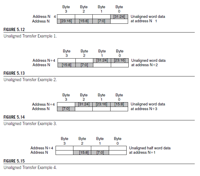
The Cortex M3 supports unaligned transfers on signle accesses. Data memory accesses can be defined as algined or unaligned. Tranditionally, ARM processors allows only aligned ransfers. That means in accesing memory, a word tranfer must have address bit[1] and bit[0] equal to 0, and a half word transfer must have addres bit[0] equal to 0. For example, word data can be located at 0x1000 or 0x1004 but it cannot be located in 0x1001,1002, or 0x1003. For half word data, the addres can be 0x1000 or 0x1002, but it cannot be 0x1001.
So, what does an unaligned transfer look like? Figures 5.12 through 5.16 show some examples
- Unaligned transfers are not supported in load/store multiple instructions.
- stack operation(push/pop) must be aligned
- Exclusive accesses (such as LDREX or STREX) must be aligned; otherwise, a fault exception(usage fault) will be triggered.
- Unaligned transfers are not supported in bit-band opertions. Results will be unpredictable if you attempt to do so.
When unaligned transfer are used,they are actually converted into multiple aligned transfers by the processor's bus interface unit. This conversion is transparent, so application programmers do not have to worry about it. However, when an unaligned transfer takes place, it is broken into separate transfers, and as a result, it takes more clock cycles for a single data access and might not be good for situations in which high performance is requred. To get the best performance, it's worth making sure that data are aligned properly.
정렬되지 않은 전송(unaligned transfer)이 사용될 때, 프로세서의 버스 인터페이스 유닛은 실제로 여러 개의 정렬된 전송으로 변환합니다. 이 변환은 투명하게 이루어지므로 응용 프로그래머들은 이를 걱정할 필요가 없습니다. 그러나 정렬되지 않은 전송이 발생하면 이는 개별 전송으로 분리되며, 결과적으로 단일 데이터 접근에 더 많은 클럭 사이클이 소요되며 고성능이 필요한 상황에는 적합하지 않을 수 있습니다. 최상의 성능을 얻기 위해 데이터가 적절하게 정렬되어 있는지 확인하는 것이 가치가 있습니다.It is also possible to set up the NVIC so that an excetion is triggered when an unaligned transfer takes place. This is done by setting the UNALIGN_TRP(unaligned trap) bit in the configuration control register in the NVIC(0xE00ED14). In this way, tje Cortex generates usage fault exceptions when unaligned transfers take place. This is useful during software development to test whether an application produces unaligned transfers.
5.7 EXCLUSIVE ACCESSES
You might have noticed that the Cortex-M3 has no SWP instruction(SWP), which was used for semaphore opertaions in traditional ARM processors like ARM7TDMI. This is now being replaced by exclusive access opertaions.
Semephores are commonly used for allocating shared resources to applications. When a shared resource can only service one client or application processor, we also call it mutual exclusion(MUTEX). In such cases, when a resource is being used by one process, it is locked to that process and cannot serve another process until the lock is released. To set up a MUTEX semaphore, a memory location is defined as the lock flag to indicate whetehr a shared resoure is locked by a process. When a process or application wants to use the resource, it needs to check whether the resource has been locked first. If it is not being used, it can set the lock flag to indicate that the resource is now locked. In traditional ARM processors, the access to the lock flag is carried out by the SWP instruction.
전통적인 ARM 프로세서에서는 세마포어 작업에 SWP(Swap) 명령어가 사용되었음을 알아채셨을 것입니다. 그러나 Cortex-M3에는 SWP 명령어가 없습니다. 이제는 독점 액세스(exclusive access) 작업으로 대체되고 있습니다.It allows the lock flag read and write to be atomic, preventing the resource from being locked by two processes at the same time.
In newer ARM processors, the read/write access can be carried out on separated buses. In such situations, the SWP instructions can no longer be used to make the memroy access atomic because the read and write in a locked transfer sequence must be on the same bus. Therefore, the locked transfers are replaced by exclusive accesses. The concept of exclusive access operation is quite simple but different from SWP; it allows the possibility that the memory location for a semaphore could be accessed by another bus master or another process running on the same processor.
To allow exclusive access to work properly in a multiple processor environment, and additional hardware called "exclusive access monitor" is required. This monitor checks the transfers toward shared addree locations and replies to the processor if an exclusive access is success.
If the memory device has been accessed by another bus master between the exclusive read and the exclusive write, the exclusive access monitor will flag an exclusive failed through the bus system when the processor attempts the exclusive write. This will cause the return status of the exclusive write to be 1. In the case of failed exclusive write, the exclusive access monitor also blocks the write transfer from getting to the exclusive access address.
다중 프로세서 환경에서 독점 액세스가 제대로 작동하려면 "독점 액세스 모니터(exclusive access monitor)"라는 추가 하드웨어가 필요합니다. 이 모니터는 공유 주소 위치로의 전송을 확인하고 독점 액세스가 성공한 경우 프로세서에 응답합니다. 프로세서의 버스 인터페이스는 또한 이 모니터에게 전송이 독점 액세스인지를 나타내는 추가적인 제어 신호를 제공합니다.
Exclusive access instructions in the Cortex-M3 include LDREX(word), LDREXB(byte), LDREXH(half word), STREX(wrod), STREXB(byte), STREXH(half word). A simple example of the syntax is as follows :
LDREX <RxF>, [Rn, #offest]
STREX <Rd>, <Rxf>,[Rn, #offset]
Where Rd is the return status of the exclusive write(0 = success and 1 = failure ).
When exclusive accesses are used, the internal write buffers in the Cortex-M3 bus interface will be bypassed, even when the MPU defines the region as bufferable. This ensures that semaphore information on the physical memory is always up to date and coherent between bus masters. SoC designers using Cortex-M3 on multiprocessor systems should ensure that the memory system enforces data coherency when exclusive transfers occur.
5.8 ENDIAN MODE
The Cortex-M3 supports both litte endian and big endian modes. However, the supported memory type also depends on the design of the rest of the microcontroller ( bus connections,memory controllers, peripherals, and so on). Make sure that you check your microcontrollers will be little endian. With developing your software. In most case, Cortex-M3 based microcontrollers will be little endian. With little endian mode, the first byte of a word size data is stored in the least significant byte of the 32-bit memory location(see table 5.4).
There are some microcontrollers that use big endian mode. In such a case, the first byte of a word size data is stored in the most significant byte if the 32 bit address memory location.
The memory view of both schemes is th e invariant big endian is supported on ARM architecture v6 and v7. The memory view of both schemes is the same, but the byte lane usage on the bus interface during data transfers is different.
