the ARM Cortex-M3 Processor - 5
Chapter 6 Cortex-M3 Implementation Overview
6.1 THE PIPELINE
The Cortex-M3 processor has a three-stage pipeline. The pipeline stages are instruction fetch, instruction decode, and instruction execution.
Some people might argue that there are four stages because of the pipeline behavior in the bus interface when it accesses memory, but this stage is outside the processor, so the processor itself still has only three stages.
When running programs with mostly 16-bit instructions, you will find that the processor not fetch instructions in every cycle. This is becuase the processor fetches up to two instructions in one go, so after one instruction is fetched, the next one ins already inside the processor. in this case, the processor bus interface may try to fetch the instrcution after the next of, if the buffer is full, the bus interface could be idle. Some of the instructions take multiple cycles to execute; in this case, the pipeline will be stalled.
In executing a branch instruction, the pipleine will be flushed . The processor will have to fetch instructions from the branch destination to fill up the pipeline again. However, the Cortex-M3 processor suppors a number of instructions in v7-M , so some of the short distance brancehs can be avoided by replacing then with conditional execution codes.
Because of the pipeline nature of the processor and to ensure that the program is compatible with Thumb codes, the read value will be the address of the instruction plus 4, when the program counter is read during instruction execution. If the program counter is used for address generation for memory accesses, the word aligned value of the instruction address plus 4 would be used.
프로세서의 파이프라인 구조와 Thumb® 코드와의 호환성을 보장하기 위해, 명령어 실행 중에 프로그램 카운터(program counter)가 읽혀질 때 읽은 값은 명령어의 주소에 4를 더한 값입니다. 메모리 액세스의 주소 생성에 프로그램 카운터를 사용하는 경우, 명령어 주소에 4를 더한 워드 정렬 값이 사용됩니다. 이 오프셋은 16비트 Thumb 명령어와 32비트 Thumb-2 명령어의 조합과는 상관없이 일정합니다. 이는 Thumb과 Thumb-2 간의 일관성을 보장합니다.Inside the instruction prefetch unit of the processor core, there is also an instruction buffer(see Figure 6.2). This buffer allows addtional instructions to be queued before they are needed. This buffer prevents the pipeline being stalled when the instruction sequence contains 32-bit Thumb-2 instructions that are not word aligned. However, this buffer does not add an extra stage to the pipeline, so it does not increase the branch penalty.
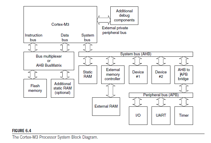
6.2 A DETAILED BLOCK DIAGRAM
The Cortex-M3 processor contains not only the processor core but also a number of components for system management, as well as debugging support components( see Figure 6.3). These components are linked together using an Advanced High Performance Bus, and an Advanced Peripheral Bus(APB). The AHB and APB are part of the Advanced Microcontroller Bus Architecture(AMBA) standers.
Note that the MPU, WIC, and ETM blocks are optional blocks that can be included in the microcontroller system at the time of implementation.
The Cortex-M3 processor is released as a processor subsystem. The CPU core itself is closely coupled to the interrupt controller (NVIC) and various debug logic blocks:
- CM3Core : Te Cortex-M3 core contains the registers, ALU, data path and bus interface.
- NVIC : The NVIC is a built in interrupt controller. The number of interrupts is customized by chip manufacturers . The NVIC is closely coupled to the CPU core and contains a number of system
6.3 BUS INTERFACES ON THE CORTEX-M3
Unless you are desinging an SoC product using the Cortex-M3 processor, it is unlikey that you can directly acces the bus interface signals described here. Normally, the chip manufacturer will hook up all the bus signals to memory blocks and peripherals, and in a few cases, you might find that the chip manufacturer connected the bus to a bus bridge and allows external bus systems to be connected off chip. The bus interfaces on the Cortex-M3 processor are based on AHB Lite and APB protocols, which are documented in the AMBA Specification.
6.3.1 The I-CODE Bus
The I Code bus is a 32-bit bus based on the AHB-Lite bus protocol for instruction fetches in memory regions from 0x00000000 to 0x1FFFFFFF. Instruction fetches are performed in word size, event for 16 bit Thumb instructions. Therefore, during execution, the CPU core could fetch up to two Thumb instructions at a time.
-> 명령어 읽기
6.3.2 The D-Code Bus
The D-Code bus is a 32-bit bus based on the AHB-Lite bus protocol; it is used for data access in memory regions from 0x00000000 to 0x1FFFFFFF. Although the Cortex-M3 processor supports unligned transfers, you won't get any unaligned transfer on this bus, becuase the bus interface on the processor core convers the unaligned transfers intoaligned transfers for you. Therefore, devices(such as memory)that attach to this bus need only support AHB-Lite aligned transfers.
6.3.3 The System Bus
The system bus is a 32-bit bus based on the AHB-Lite Bus Protocol; it is used for instruction fetch and data access in memory regions from 0x20000000 to 0xDFFFFFFFF and 0xE01000000 to 0xFFFFFFFF. Similar to the D-code bus, all the transfer on the system bus are aligned.
6.3.4 The External PPB
The External PPB is a 32 bit bus based on the APB bus protocol. This is intended for private peripheral accesses in memory regions 0xE0040000 to 0xE00FFFFF. However, since some part of this APB memory is already used for TPIU, ETM, and the ROM table , the memory region that can be used for attaching extra peripherals on this bus is only 0xE0042000 to 0xE00FF000. Transfers on this bus are word aligned.
6.3.5 The DAP Bus
The DAP bus interface is a 32-bit bus based on an enganced version of the APB specificaiton. This is for attaching debug interface blocks such as SWJ-DP or SW-DP. Do not use this bus for other purpose. More information on this interface can be found in chapter 15, or in the ARM document CoreSignt Technology System Design Guide.
6.5 The EXTERNAL PPB
Table 6.2
| Signal Group | Function |
|---|---|
| Multiprocessor communication (TXEV,RXEV) | Simple task synchronization signals between multiple processors |
| Sleep signals(SLEEPING, SLEEPDEEP) | Sleep status for power management |
| Interrupt status signals(ETMINTNUM, ETMINSTATE, CURRPRi) | Satus of interrupt operation, for ETM operation and debug usage |
| Reset request | Resets requeset output from NVIC |
| Lockup and Halted status(LOCKUP, HALTED) | Indicate that the processor core has entered a lockup state(casused by error conditions within hard fault handler or Nonmaskable interrupt handler) or a halted state(for debug operations) |
| Endian input(ENDIAN) | Sets the endian of the Cortex-M3 when the core is reset connects to ETM for instruction trace |
| ETM interface | Connects to ETM for instruction trace |
| ITM's ATB interface | ATB is bus protocol in ARM's CoreSight debug architecture for trace data transfer; here this interface provides race data output from Cortex-M3's ITM, which is connected to the TPIU |
This bus interface supports the use of CoreSight compliant debug components. To achieve this, this interface is slightly different from normal APB-it contains an extra signal called PADDR31 that indicates the source of a transfer. If this signal is 0, it means that the transfer is generated from software running on the Cortex-M3.
If this signal is 1, it means that the trnasfer is generated by debugging hardware. Based on this signal, a peripheral can be disigned so that only a debugger can use it, or when being used by software, onyl some of the features are allowed.
6.6 TYPICAL CONNECTIONS
Because there are a number of interfaces on the Cortex-M3 processor, you might find it confusing to see how it will connect with other devices such as memory or peripherals.
Since the Code memory region can be accessd by the instruction bus(if it is an instruction fetch) and from the data bus(if it is a data access), an AHB bus switch called the BusMatrix or an AHB bus multiplexer is needed.With the Bus Matrix, the Flash memory and the additional SRAM can be accessed by either bus interface. The BusMatrix is available from ARM in the AMBA Design Kit(ADK). When both data bus and instruction bus are trying to access the same memory device at the smae time, the data bus and instruction bus are trying to access the same memory device at the same time, the dat abus access could be given higher priority for best performance.
Using the AHB Bus Matrix, if the instruction bus and the data bus are accessing different memory devices at the same time(for example, and instruction fetch from fetch and a data bus reading data from the additional SRAM), the transfers can be carried out simultaneously. If a bus multiplexer is used, however, the transfers cannot take place at the same time, but the circuit size would be smaller. Common Cortex-M3 microcontroller designs use system bus for SRAM connection.
AHB BusMatrix를 사용하면, 명령어 버스와 데이터 버스가 동시에 다른 메모리 장치에 접근하는 경우(예: 명령어 버스에서 명령어를 가져오고 데이터 버스가 추가 SRAM에서 데이터를 읽는 경우) 전송은 동시에 수행될 수 있습니다.아~ 그래서 SRAM에 스택 Heap 영역 할당하고 IROM으로 코드 실행시키는 구나
The main SRAM block should be connected through the system bus interface,using the SRAM memory address region. This allows data access to be carried out at the same time as instruction access. It also allows setting up of Boolean data types by using the bit-band feature.
Some microcontrollers might have an external memory interface. That requries an external memory controller becuase you cannot connect off chip memory devices directly to AHB.
The external controller can be connected to the system bus of the Cortex-M3. Additional AHB devices can also be easily connected to the system bus without the need for a BusMatrix.
Simple peripherals can be connected to the Cortex-M3 through an AHB to APB brdige. This allows the use of the simper bus protocol APB for peripherals.
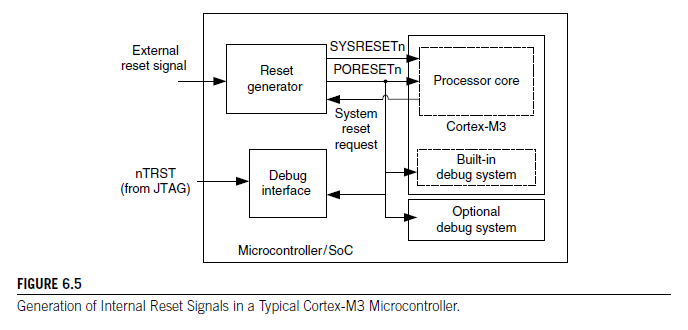
6.7 RESET TYPES AND RESET SIGNALS
There are a number of different reset types on a Cortex-M3 system. Some Cortex-M3 product might have more reset types depending on the design of reset circuitry on the Cortex-M3 microcontroller or SoC.
Table 6.3
| Reset Type | Reset Signal on the Cortex-M3 Processor | Description |
|---|---|---|
| Power on reset | PORESETn | Reset that should be asserted when the device is powered up; resets processor core,peripherals, and debugging system |
| System reset | SYSRESETn | System reset; affects the whole system including processor core, NVIC(except debug control registers), MPU, peripherals but not the debugging system; activate by power up sequence of the device,reset request from debugger through NVIC register "AIRCR" |
| Processor reset | VECTRESET bit in the NVIC AIRCR register | Reset processor core only; affect the processor system including processor core, NVIC(except debug control registers),MPU,but not the debugging system; activate reset request from debugging system; |
| JTAG reset | nTRST | Reset for JTAG tap controller(only if JTAG interface is availalbe) |