디지털 회로 개론 23 (ASIC and CAD, Circuit Classification, Circuit design, Circuit Design Constraints)
20) 디지털회로개론
ASIC (Application Specific Integrated Circuit) and CAD
ASIC : 특정 기기를 위한 특별한 회로로 시장이 수요가 충분히 커야지 만들어 낼 수 있다.
그래서 다음의 사항들을 고려하게 된다.
- volume of sales
- fast design time
- low design cost
- design quality measured by performance and manufacturing yield
Circuit Classifications
- semiconductor materials:
- silicon onsapphire, or p-well and n-well
- Gallium-arsenide 순으로 사용된다.
- electronic device types
- CMOS(Complementart Metal Oxide Semiconductor) : PMOS and NMOS
- Bipolar
- Combination of CMOS and Bipolar : BiCMOS
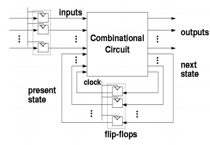
- Digital circuits in mode of operations
- Synchronous circuit
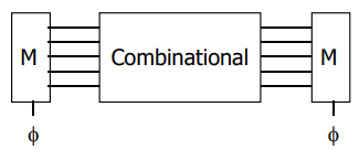
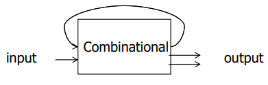
clock이 칩 전체에 퍼져있어야 하는데 그게 상당히 복잡하고 문제가 생기기 때문에 디자인하는데 어렵다. 그리고 clock이 전력소모가 상당히 크다. 하지만 가장 일반적으로 사용되는 회로이다. - Asynchronous circuit
- Synchronous circuit
- Microelectronic Design Styles
- custom design
- semi-custom design
우리가 회로를 설계하는 방법에는 아래 4가지가 존재하는데 거기에서도 트랜지스터에 디자인 되는 방식이 두가지가 존재한다.
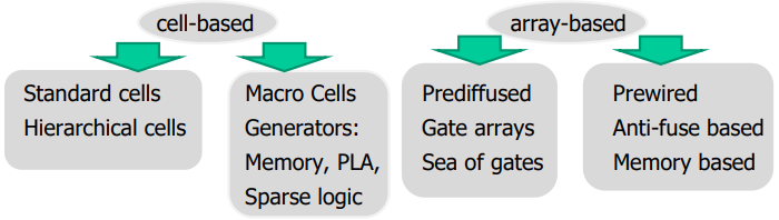
cell-based는 하나하나의 게이트를 디자인 한다. array-based는 적인 구조를 어떻게 연결해서 프로그래밍할지에 대해 이야기 한다.
Cell based design
- Standard-cell design
standard library를 가져다가 mapping을 해서 제작한다.
Macro-cell based design
메크로 셀을 제공해서 여러개의 and와 or 게이트를 제공해주는 macro-cell based design이다.
Array based design
- Prediffused(mask programmable) based design
- Gate Arrays
- Prewired(field programmable gate arrays) based design
- Anto-fuse based
- memory based
custom으로 제작하면 굉장히 비싸고 많은 시간이 걸리기 때문에 다른 방식의 디자인 스타일을 구해내곤 한다.
Circuit design
- design
보통 Hardware Description Language로 구현된다.
verilog를 사용하여서 칩으로 만들기 위하 단계까지 넘기어 줄 수 있다.
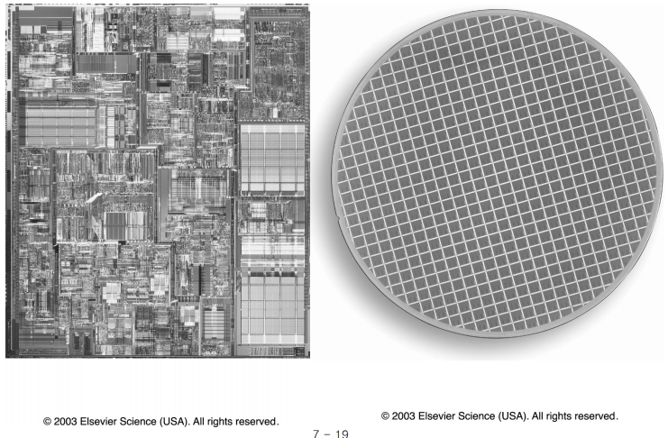
Pentium 4 microprocessor die and 8-inch wafer
Design Flow Example
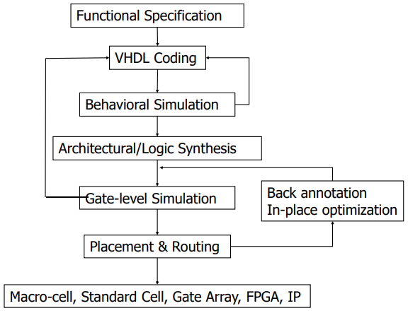
위의 과정으로 회로를 디자인 하게 된다.
System-On-Chip
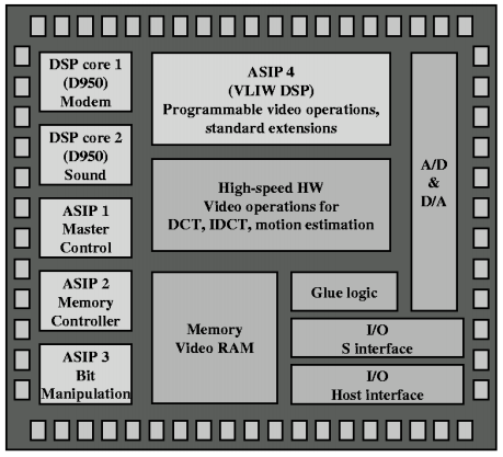
최종적으로 위와 같은 칩을 만들 수 있게 된다.
Circuit Design Constraints
-
Performance
– Timing models (RC delay, table model, non-linear equations) -
Area
– Size shrinks due to technology improvement -
Power
– 3 types of power consumption
• Dynamic
• Short circuit
• Leakage -
Testability
-
Design time
-
Cost
-
Yield
회로를 디자인 할때 위의 7가지 특히 1-3번이 가장 회로에서 중요한 역활을 하게 된다.
Performance constraint
Timing analysis
– Entire chip
– Critical path

FF 사이에 있는 로직들이 얼마만큼의 Worst Case Delay를 가지는가
– Block
– Latch (setup and hold time)
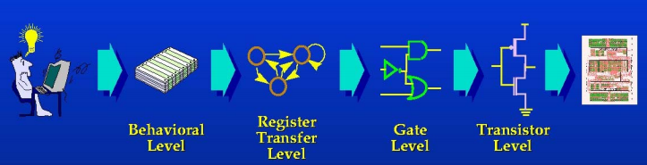
3 levels of analysis
– Transistor(Switch)-Level , Logic(Gate)-Level, High-Level
Performance analysis - Gate level
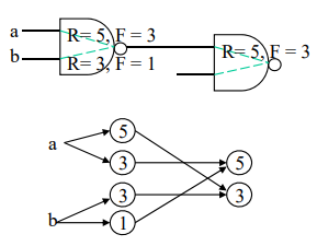
Input이 들어왔을 때 각각의 입력에 따라 Delay가 어떻게 변화하고 Worst Case Delay를 계산하는 것을 이야기 한다.
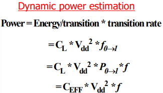
Power
DEC Alpha 72W, Pentium Pro 40W
Computer aided design for power
요즘에는 Power을 어떻게 하면 덜 들 수 이쎅 할 수 있을지를 연구한다.
Source of power consumption
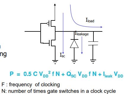
Dynamic Power Consumption
- Charging and Discharging Capacitors
- 회로를 가지고 연산을 하거나 로직 함수를 실행을 시킬때 소비되는 power consumption
Short Circuit Currents
- short circuit path between supply rails during switching
Leakage (static power consumption)
- Leaking diodes and transistors
- 우리가 회로를 아예 배터리에서 분리시커 놓지 않으면(아예 차단방법은 이것밖에 없다) 회로가 아무일도 하지 않을 때 누수 전류가 발생한다.
Gate-level power estimation