1.
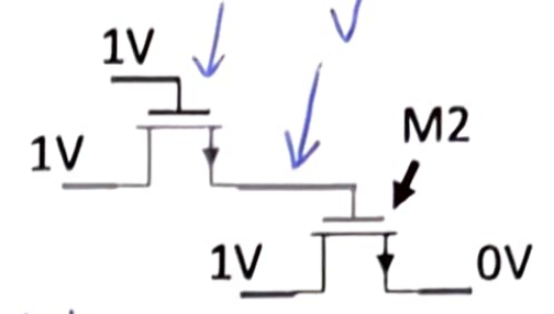
Two NMOS are connected as shown here. What mode of operation (cutoff, linear, saturation) is M2 in? Vt for both MOS is 0.6V. Useful info: The side with the arrow is the source side, Cutoff: Vgs<Vt, Linear: Vgs>Vt & Vds<Vgs-Vt, Saturation: Vgs>Vt & Vds>Vgs-Vt)
2.
For some application, it is desired that the high-to-low transition must be high speed while the low-to high transition is of little consequence. What change(s) will you make to your inverter to account for this requirement?
3.
Implement the Pull-down-network (PDN) only, for the function:
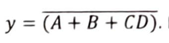
No need to size.
4.
For a new Technology, it was determined that 1:2 sizing is optimal(Not 2:1). with this new information. size your design from Q3.
5.
Given the following PDN (Assume that there is also a complementary PUN, that is not showed here), what will be the output(0 or 1) when inputs are
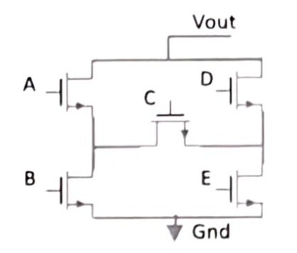
a. (A,B,C,D,E) = (1,1,0,0,0): Output:0
b. (A,B,C,D,E) = (1,0,1,0,1): Output:0
c. (A,B,C,D,E) = (1,0,1,1,0): Output:1
6.
Between a 2-input NAND and 2-input NOR, which will consume more dynamic power and why (voltage, and frequency are equal in both cases, the output of both gates is connected to 2:1 inverters)?
(Useful info: Paynamic = aCV'f, a: Switching factor, C: load capacitance, V: Voltage, f; frequency)
The NOR gate requires larger PMOS transistors because its PMOS devices are connected in series, which increases the switched capacitance and therefore increases dynamic power.
7.
What is the logical (LE) for a 2-input NAND and 2 input NOR gate if 3:1 sizing is followd in a new technology. Useful info: LE is the ratio of the input capacitance of a given gate to that of an inverter after sizing.
8.
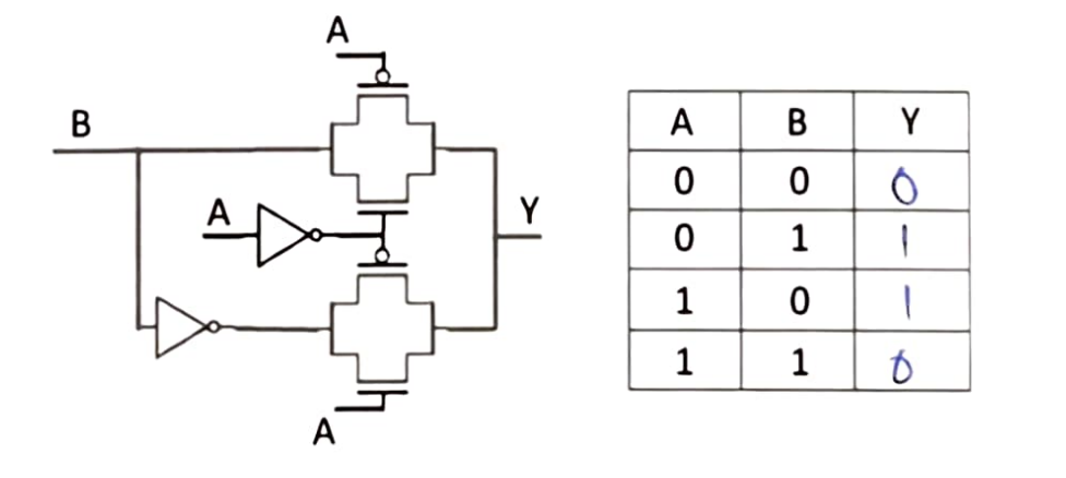
Fill up the truth table for the following circuit. What function is being implemented?