When the processor enters sleep mode, the power management unit dectects the sleep operation and then requests to change the processor to low-power state by asserting QREqn to 0. The processor can then drive QACCEPTn low tp omdocate that the low power state request is accepted.
After the processor accepts the low power mode request, it then puts the processor in the targeted low power state(i.e., SPRG),
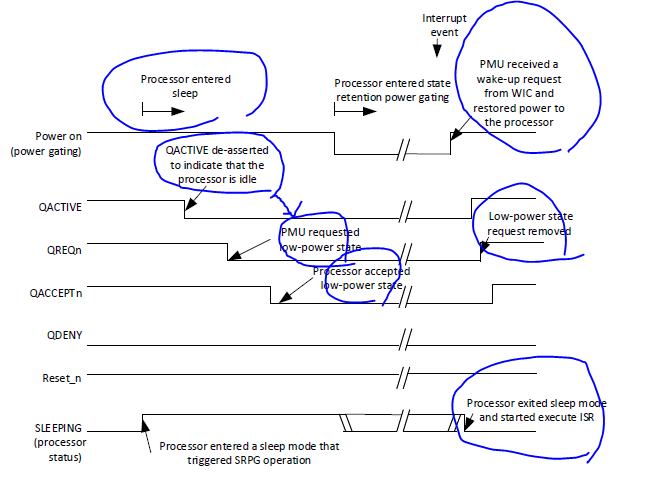
Assuming that the processor system has a Wakeup Interrupt Controller in an always-on power domain or similar hardware features, then a peripheral activity triggering an interrupt requeset can wake up the system via a separate connection netween the WIC and the power management. In this scenario, the power management controller can resotre the power and clock signal activity to the processor system, and then the Q-channel can complete its handshaking sequecne
If an interrupt request arrives just after the processor has entered sleep mode, then it is possible for the processor to reject low power satte requeset using the QDENY siganl. In such cases the PMU must not power down the processor in order to allow it to continuse uts operations
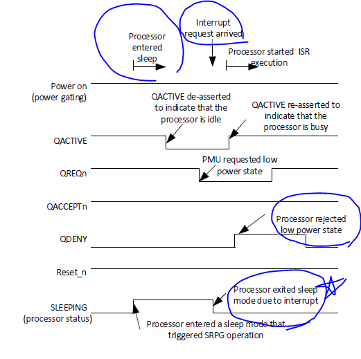
-> 슬립 도중에 interrupt 가 들어오면 QDENY 로 LOW power 모드 다시 안한다고 요청한다.
It is possible that some power domains of a processor can start up in a low-power state. For example, the debug power domain of a processor can be in an OFF state when the system starts and turned on only when a debugger is connected. In such cases, the QACTIVE and QREQn signals will have a start up level of zero instead of one.
In addition to processor systems, the Q-channel can also be used in other system componets. Since the handshake protocol is fairly simple and is very generic, it can be deployed for many components of a low power microcontropller or system-on-chip design.
6.3.3. sleep hold interface
The sleep hold interface is used to delay the resume of program execution when the processor wakes up from a sleep mode. There would be various reasons for using this interface: one example is that a memory block might need some clock cycles to get itself out of low-power states. Please note this feature is less likey to be used when the WIC is used because it is possible to hold the processor in sleep mode by gating off all colcks while detection is handled by the WIC.
The sleep hold interface contains two signals :
| signal name | Description |
|---|---|
| SLEEPHOLDREQn | Input of processor. When using this feature, set this signal to 1 after entering sleep mode. |
| SLEEPHOLDACKn | Output from processor to indicate sleep hold request is accepted |
These two signals are active-low and interface with a power management unit(PMU) or the system controller developed by silicon vendors.
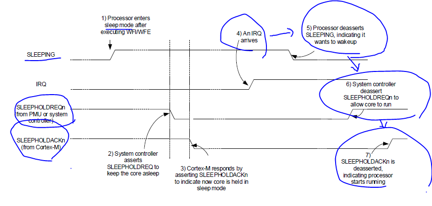
The operation of the sleep hold interface is very simple : When the PMU or system controller detects that the processor core has entered sleep(SLEEPING or SLEEPDEEP signals), it can then assert the SLLEPHOLDREQn signal to the processor. If the processor core responds with the assertion of SLEEPHOLDACKn(pulled low), then the PMU or system controller can then reduce the power by turning off the flash memories, peripherals, PLL etc. If the processor core does not respond with SLLEPHOLDACKn, then it means the processor core might have received an interrupt or a debug request, so it is going to wake up. In this case, the PMU or system controller should not carry out any further action and de-assert SLEEPHOLDREQn when sleep signals is de-asserted.
If the sleep hold request has been accepted after the system has entered sleep, and an interrupt arrives, the processor core will de-assert the sleep signals. However, the processor core will not resume program excution until SLEEPHOLDREQn from PMU or system controll is de-asserted.
When the flash memory voltage supply is resumed, and all the logic is ready, the SLEEPHOLDREQn can be de-asserted, and the execution of the interrupt service routine can be started.
During the extended sleep, it is possible to stop the HCLK if GATEHCLK is high.
If the sleep hold feature is not needed, the SLEEPHOLDREQn input signal can be tied high.
6.3.4 Wakeup Interrupt Controller(WIC)
If a Cortex-M processor has all of its clock signals gated off or has been pu into a state retention power down state, then its NVIC will not be able to dectect incoming interrupts or other wake-up events. To solve this problem, the WIC feature was introduced.
The WIC is an optional block that is in a separated always on the power domain that wil ltake the role of interrupt and wake up event decteion when the BNVIC is stopped or powered down. The exact interface and integration details cna be perocessor-specific. In general, the interface between the WIC and processor contains:
| Signal name | Direction | Description |
|---|---|---|
| WICMASKxxx[n:0] | Processor to WIC | Wakeup event mask. Contain mask status for NMI, RXEV, EDBGRQ(for Armv7-M, Armv8-M Mainline) and IRQ signals. The signal width is configurable. |
| WICLOAD | Processor to WIC | Indicate to WIC that the WICMASK is valid and needs to be captured |
| WICCLEAR | Processor to WIC | Clear the wake-up event mask inside WIC |
The WIC has the following outputs to the system :
|signal name | direction | description |
|---|---|---|
|WICINT[n:0]/IRQ + other wake up events | input | Wakeup events : NMI, RXEV, EDBGRQ and IRQ signals. The signal width is confugurable |
|WAKEUP|Output | Wakeup request to the system controller to indicate that the processor needs to be woken up to serve an interrupt request or other event. |
|WICPENDxxx[n:0] | Output | Latced version of an interrupt request. Since the incoming interrupt event could be single-cycle, the WIC holds the request status until the processor is back operating and WICCLEAR is asserted. This can be fed to NVIC's interrupt inputs vis an OR logic.|
Finally, there can be an additional interface on the Cortex-M processor to enable/disable the WIC operation
The WIC deliverd in the Cortex-M product bundle is an example of this small interrupt detection logic, and it is modifiable. In some cases, designers have modified the WIC to enable a latch-based operation so that wake-up events can be detected and captured without any active clocks.
An overview of the WIC operations is as follows:
When entering sleep mode, the wakeup event mask is transferred from NVIC to WIC using a dedicated hardware interface(WICMAKS[] and WICLOAD).
When a wake-up event is detected, the WIC sends a wake-up request to the system power management control.
The power management control then restores the power to the processor and resumes clocking. The processor can pick up the interrupt request(or other wake up events) and resume operation.
The wake-up masking information and pending wake-up event held inside the WIC is cleared by hardware automatically when the processor processor wakes up from sleep mode(WICCLEAR).
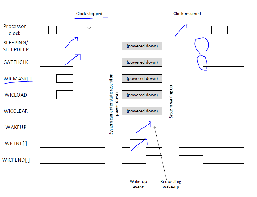
Figure 6.11: Simplified wakeup interrupt controller operations.
Wake-up event 가 발생하고 Wakeup 되고 Pending 없어지고
Clock 발생 되고 SLEEP , GATEHCLK de-assertion 되고
In Cortex-M0, Cortex-M0+, Cortex-M3, Cortex-M4 , Cortex-M7, and Cortex-M23 processors, the WIC is external to the processor.In Cortex-M33 and Cortex-M35P , the WIC is intergrated inside the processor. In different Cortex-M processors, the handling of wakeup event routing is slightly different:
In Cortex-M3 and Cortex-M4, the merging of a pending wake-up event with the original source is out side of the WIC. This is merged into the WIC in newer Cortex-M processor designs.
In different Cortex-M processors, the handling of wakeup event routing is slightly different :
In Cortex-M3 and Cortex-M4 , the merging of a pending wake up event with the original source is outside of the WIC. This is merged into the WIC in newer Cortex-M processor desings.

In Armv7-M or Armv8-M Mainline processor systems, the EDBGRQ signal ( external debug request) is included as one of the wake-up events that the WIC monitors. This is because the external debug request can trigger a Debug Monitor exception if it is enalbed. In Arm6v-M and Armv80M baseline systems(i.e., Cortex M23 processor system), the EDBGRQ is not considered to be a wake-up event as the Debug Monitor exception is not available.
The WIC feature can be enabled or disabled with a handshaking signal interface. In the Cortex-M3 and Cortex-M4, this interface involves a pair of handshaing signals between the processor and the WIC, and another pair of handshaking signals between the WIC and the system-level control registers (device-specific).
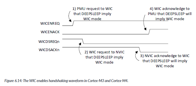
At the start of the application, the software can write to a regitster in the system power manangement unit(outside of the processor, device-specific) to enable the WIC feature. This enables the power management unit that handles state retention power gating. The WIC is ten ebalbed with the following handshaking sequence :
In later Cortex-M processor design, the WIC enable/disable interface is simplifed so that it only needs the WICENREQ and WICENACK signals. there is no need for additional handshking between the WIC and the processor.
When using State Renteion Power Gating, the system desiner will need to handle a number of control signals. The control sequence of these signals are process node-specific. In a simple example, you might see the follwing signals :
| signal | Description |
|---|---|
| ISOLATEn | Use to isolate the power domain |
| RETAINn | Use to control, retain and restore state retention logic cells |
| POWERDOWN | Power down control for power gating |
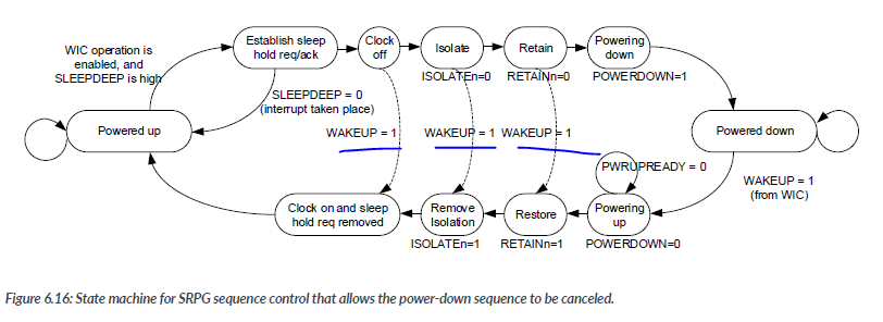
System designers need to create a state machine to control the sequence for entering the power down state and exiting from the power-down state. To support thse operations, the power management design also needs to include a status signal to indicate if the power-up has been done( let us assume that this signal is called PWRUPREADY in the following state machine diagrams). When in the power-down state, the WAKEUP signal from the WIC is used to switch the state machine into the wake-up sequence.
Silicon vendor might choose different approaches to develop their power control FSM. For example, the FSM can optionally allow the power down sequence to be canceled if the WAKEUP signal is aserted before being powered down to reduce the interrupt latency(Figure 6.16).
-> WIC operaion is ebalbed, and SLEEPDEEP is high -> Establish Sleeop hold req/ack -> clock off -> isolate -> retain -> powering dwon
6.3.5 SRPG's impact on software
The SRPG feature can greatly reduce the power consumption of sleep modes. However, there are a few areas that application dvelopers must be aware of :
-
The SYSTICK timer will be stopped during power down. As the processor is powerd down, the SYSTICK timer inside the processor would be stopped. Embedded applications that use OS will need to use a time external to the processor core to wake it up for task and event scheduling.
Sleep modes that still allow free running processor clocks should not be affected - embedded application programmers should check the sleep mode details from chip manufacturers. -
The interrupt latency is increased when WIC or SRPG is used. Since it will take a certain duration to power up the processor, memories, and get the system ready, the interrupt latency can be increased substantially.
-
Powerdown is normally disabled when a devugger is attached. This is because debuggers require access to the processor even when the processor core is in sleep modes. In many such cases, the power down FSM is automatically disabled by the WIC interface inside the processor. As a result, testing of deep sleep can show a different set of behaviors and interrupt latency when a debugger is connected.
6.3.6 Software power saving approach
One of the considerations in software devleopment is to decide whether to :
Run fast and enter sleep mode as much as possible, or,
Run slow to reduce dynamic power.
Unfortunately, there is no golden rule. If the oscillators use large amounts of power, running them slowly might be a good way to reduce power consumption. However, this also has the effect of increasing interrupt latency and overall leakage current.
On the other hand, if the flash memories have a high leakage current, run fast and sleep( while also turning off the flash memory). this could be a good wayto reduce overall energy consumption. However, it means that the peak power will be higher.
6.4 Cortex-M processor characteristics that enable low-power designs
6.4.1 High code density
Since the Cortex-M series of processors uses a mixture of 16-bit and 32-bit instructions in its instruction set, it enables high code density, which means an application could fit into a smaller program ROM/flash size.
High code density can have various advantages. In addition to opportunities to reduce power by using a smaller program ROM/flash, it can also help to :
Reduce cost;
Enalble small chip packages.
6.4.2 Short pipeline
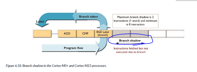
Most of the Cortex-M processors(except Cortex-M7) have a fairly short pipeline(2 to 3 stages). In these processor desings, the short pipeline nature enables the processor to have a low branch penalty without having to include branch prediction logic.
The shorter pipeline also reduces branch shadows which are instructions after a branch that are fetched by the processor but are discarded if the branch is taken. For example, in the Cortex-M0+ and Cortex-M23 processors, as the pipeline is only 2 stages long, the branch shadow is reduced to just one word. Branch shadows are bad for energy efficiency as they mean that the memory system has used energy to fetch the instructions, but those instructions are not needed.
6.4.3 Instruction fetch optimizations
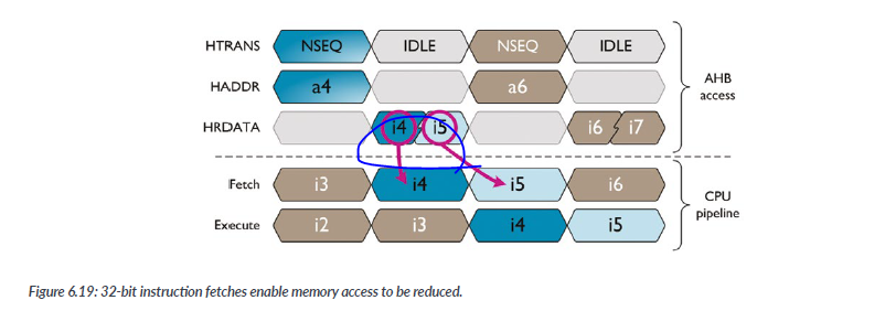
While some of the instructions are 16-bit, the Cortex-M processor fetches instructions as 32-bit most of the time(or 64-bit for Cortex-M7 when using 64-bit I-TCM or AXI interface). It means for each instruction fetch, it could obtain up to 2 instructions, and the instruction fetch interface can be idle some of the time to reduce power spent on program memory access.
The Cortex-M0_ and Cortex-M23 processors also support halfword instruction fetches if a branch target is not word-aligned(bit 1 or address is 1). It means half of the byte lanes for that access can be inactive and could save quite a bit of power in short loops.
6.5 System-level design considerations
6.5.1 Low-power designs overview
Low-power design is a verylarge topic. In addition to utilizing different sleep modes of the processors or extending that to extra sleep modes, all parts of the chip can have an impact on low power capability and energy efficiency. Typically, clock gating is used in many parts of a micocontroller's design, and if possible, some of the peripherals can also be powered down when they are not being used.
6.5.2 Clock sources
A low-power clock source is one of the key items. Many designs need to have a 32KHz clock that is always on(for real time clock and power management), and if this clock source is power hungry, it would have a big impact. Ideally, the 32kHz clock source needs to be ultra-low-power,accurate, and capable of working with wide voltage ranges.
Selection of crystal operation range is also important. While a microcontroller product might be designed to run at 100MHz, having a 100Mhz crystal in the desgin means the product will have a 100MHz clock runnung all the time and can burn a lot of power. Therefore, it is common to use a relatively slow crystal(4 to 12Mhz) and use PLL to generate higher clock frequencies only if they are needed.
-> 일반적은 적은 속도의 크리스탈을 사용하고 PLL 을 통해 고주파수 클락을 생성함.
6.5.3 Low-power memories
Many memory macros have various sleep/retention modes and a range of 'hooks' to allow system designers to link the memory low-power states to the system's sleep modes. PLase note that there are trade-offs between sleep mode power and wake up latency
For embedded flah, it is also possible to power down the flash completly during sleep as there is no issue of data loss. However, when doing this, be aware of the in rush current when the falsh macro si turned on. which potentially can cause a voltage drop in power rails and result in problems affecting other parts of the chip.
Some devices might allow the softare to wrtie to flash before brwon-out so that crucial data in SRAM can be restored later. This poeration might also be needed when the battery of the product is being replaced. If a design needs to support such feature, the minimum flash programming voltage and flash power during programming can become a critical issue.
-> 메모리를 저전력 모드로 들어가게 할수 있지만 Wake up 하는데 latency 가 길수도 있다.
flash 메모리는 아예 꺼버려도 된다 sleep 모드에서
6.5.4 Caches
While adding a cache unit can increase the silicon area and the leakage current, and hence increase the power requirement of a system. sometimes it can help reduce the overall energy efficiency because it reduces the access to the main memories, especially embedded falsh, which can be power hungry. It also has the benefit of enalbing higher performance because flash memories are often quite slow.
=>
캐시 유닛을 추가하는 것은 실리콘 면적과 누설 전류를 증가시킬 수 있으며, 따라서 시스템의 전력 요구량을 높일 수 있습니다. 그러나 때로는 전체적인 에너지 효율성을 향상시킬 수 있는데, 이는 주로 전원 소모가 많은 임베디드 플래시를 포함한 주 메모리 액세스를 줄이기 때문입니다. 또한, 캐시는 플래시 메모리가 일반적으로 상당히 느리기 때문에 높은 성능을 가능하게 합니다.
6.5.5 Low power analog components
A range of analog components might need to stay on during sleep modes. These include a 32 kHz oscillator, real time clock, brown out detector, some of the I/O pads(e.g., when an input is used for external interrupt detection), etc.
Many I/O pads have configurable power modes that can reduce power by adjusting drive strengths and skew rates. SYstem designers can make these options programmable by introducint programmable registers to control these configuration sigals.
드라이브 강도(Drive Strength)는 I/O 패드에서 출력 신호를 송출하는 데 사용되는 전력의 양을 나타냅니다. 드라이브 강도는 출력 신호의 크기와 안정성에 영향을 줍니다. 일반적으로, 높은 드라이브 강도는 큰 출력 신호를 생성하고 장치 간의 통신 거리를 늘릴 수 있습니다. 그러나 높은 드라이브 강도는 전력 소비가 증가할 수도 있습니다.

스쿠(Skew)는 시간에 따른 출력 신호의 지연을 의미합니다. I/O 패드의 스쿠 효율은 출력 신호의 변화가 정확한 시점에 발생하도록 조절하는 것을 의미합니다. 스쿠가 작으면 출력 신호의 변화가 정확한 타이밍에 이루어지므로, 데이터의 안정성과 신호의 불확실성을 개선할 수 있습니다.

드라이브 강도와 스쿠 효율은 I/O 패드의 동작을 제어하는 파라미터로, 시스템 디자이너는 이를 조정하여 전력 소비와 신호의 품질을 조절할 수 있습니다. 예를 들어, 낮은 드라이브 강도와 작은 스쿠를 사용하면 전력 소비를 줄이고 노이즈를 감소시킬 수 있지만, 통신 속도나 신호 강도는 제한될 수 있습니다. 따라서 시스템의 요구 사항과 제약 사항에 맞게 드라이브 강도와 스쿠 효율을 조정해야 합니다.
6.5.6 Maximizing clock gating opportunities
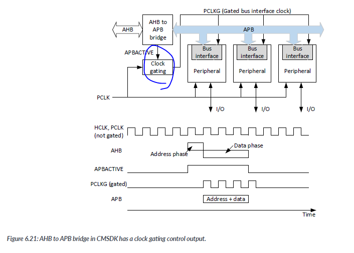
In many system designs, it is possible to place clock gating in a range of locations to reduce dynamic power. This includes peripherals and buses. For example, the AHB to APB bridge provided in Arm in the Corstone Foundation IP/ Cortex-M system Design Kit provides a clock gating control signal (APBACTIVE) to allow the down stram APB peripheral bus to be clock gated when there is nobu transaction going through.
->
클럭 게이팅은 사용되지 않는 주변장치나 버스를 비활성화하여 전력 소비를 줄입니다. 예를 들어, 버스에 트랜잭션이 발생하지 않을 때 해당 버스를 비활성화하는 것은 해당 버스의 동적 전력 소비를 크게 감소시킬 수 있습니다.
To take advantage of this feature, a peripheral might need to be modified so that it has separate clock signals for the bus interface and peripheral operations.
In some cases, the peripheral buses might be clock gated and software introduced to enable the clock on the peripheral buses before accessing the bus slaves on it.
-> 일부 경우에는 주변 버스(peripheral buses)가 클럭 게이팅될 수 있으며, 소프트웨어를 도입하여 주변 버스의 클럭을 주변 장치에 액세스하기 전에 활성화시킬 수 있습니다. 이를 통해 주변 버스는 필요할 때만 활성화되어 동적 전력 소비를 줄일 수 있습니다.
6.5.7 Sleep mode that completely powers down the processor
It is possible to completely power down the Cortex-M processor and still be able to wake up the system on certain hardware events. However, in such cases:
The processor states will be lost. Hence, software using this power down arrangement must save critiacl information to state retention SRAM beforehand.
The system design needs to have additional hardware logic to handle the hardware wake-up event detection.
If using such an approach, system designers need to add a custom-defined wake up unit to detect wakeup events, which then :
Signals to power management hardware to restore power to the porcessor system :
Resets the processor system(without resetting the state retention memories and registers);
Release resets and the processor can then boot-up and execute software.
In such a system, the design will need a few extra components :
Figure 6.22: Additional hardware needed for sleep mode with full power-down.
Power ctrl(control) - allows the software to select which sleep mode is used(e.g., wheter to enter power down when in deep sleep)
Reset info register - allows the software to decide if it is a cold boot or akeup after a power- down 'sleep'.
State retention SRAM(optional) for holding various program state information.
Wakeup event detection - enables the generation of wake-up events from peripherals of I/O. This is likely to be programmable to allow the software to decide if this is enabled or not.
Also, since the wake-up process is going to take time, the design must also hold the wakeup event information so that software can have time to enale NVIC.
Debug access port(DAP) - You might optionally move the SWJ-DP to the always-on power domain to allow the debugger to wake up the system with a debug connection. An alternative solution is to use another hardware mechanism to wakeup the system so that debugger can connect to the processor to start the debug sesstions.
The downside of this approach is that the processor must boot-up first and will, as a result, take longer time to service the interrupt. It is possible to reduce the boot time by storing most of the key processor's state into retention SRAM before powering down and restoring this after waking up.
If using this method, the sleep procedure should be handled in privileged thread mode, and if TrustZone is implemented, the sleep procedure should be in Secure privileged tread mode so that all the register states can be accessed easily.
The information that might need to be stored includes:
NVIC settings ;
MPU settings ;
Potentially SysTick settings;
Banked SP(Both MSP and PSP might be needed), and if TrustZone is implemented, all fourstack pointers and corresponding stack limit registers should be stored;
Special registers(PRIMASK, FAULTMASK,BASEPRE, etc.), - and beware that if TrustZone is present,these registers are banked and both versions will need to be saved;
FPU settings if FPU is preset, and optionally FPU registers if the FPU was used and active;
->
수면 모드에서 깨어난 후에는 저장된 상태를 복원하여 프로세서의 동작을 빠르게 재개할 수 있습니다. 이를 통해 모든 설정을 처음부터 다시 구성할 필요 없이 프로세서의 동작을 빠르게 재개할 수 있습니다.
Another thing to bear in mind is that if TrustZone is implemeted, the security management of retention SRAM is important as Secure information is stored in it when using this power down approach.
