7.1 Overview
For peripheral conncetions, APB is used in the example, and the APB bus segment is connected via an AHB to APB bridge, As explained in Section 4.5, if you are using M3 M4 M7 M33, the PPB interface is primarily for debug components and should not be used for general peripherals.
The example system that we are going to build contains a behavioral model of two memory blocks(Program ROM and RAM) and a number of simple peripherals on the APB including two parallel I/O interface ports. a UART and two simple times. In additionm a number of basi AMBA infrastructure blocks including an AHB bus bridge to APB and bus slave multiplexers will also be created.
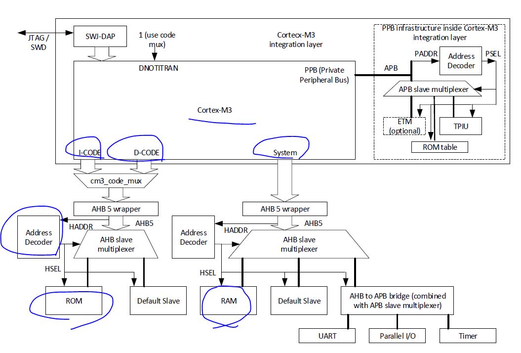
-> ROM 에는 I-CODE 와 D-CODE 로 구분되서 Cortex-M3 가 접근하고 System 은 RAM 이나 UART , Peripharal Timer 를 접근한다.
암 아키텍처에서 instruction code와 data code를 나누는 이유는 주로 성능과 보안 측면에서 설계상의 이점을 얻기 위해서입니다.

성능 향상: 암 아키텍처에서는 instruction code와 data code를 별도의 버스로 분리함으로써 동시에 명령어와 데이터를 전송할 수 있습니다. 이를 통해 동시에 명령어를 가져오고 동시에 데이터를 로드하는 등 병렬 처리가 가능해집니다. 이는 명령어와 데이터 접근이 동시에 이루어져야 하는 경우에 대한 성능 향상을 가져올 수 있습니다.

보안 강화: 암 아키텍처에서는 프로그램과 데이터를 분리하여 실행하는데, 이는 보안상의 이점을 제공합니다. Instruction code와 data code가 분리되어 있으면, 프로그램 실행 중에 데이터 영역에 대한 액세스를 제한할 수 있습니다. 이는 악성 코드가 실행 중에 프로그램 데이터를 손상시키는 것을 방지하고 시스템의 안전성을 높일 수 있습니다.

또한, Instruction code와 data code를 분리함으로써 명령어와 데이터를 별도로 캐시에 저장할 수 있습니다. 이는 캐시 메모리의 효율성을 높이고 성능을 향상시키는 데 도움이 됩니다.

요약하자면, 암 아키텍처에서 instruction code와 data code를 별도의 버스로 분리함으로써 성능 향상과 보안 강화를 이루고, 병렬 처리와 캐시 메모리의 효율성을 높일 수 있습니다.
This example system has the following characteristic :
Two default slaves are needed as there are two AHB bus segments, each of them containing invalid address ranges
DONTITRAN input(applicable for Cortex-M3 and Cortex M4 processors only) is set to 1 because we are using a code mux module to merge I-CODE bus and D-Code
In this design, the APB slave multiplexer and AHB to APB bridge are combined, it is also absolutely fine to separate the two functions into two modules.
- The PPB bus connections are handled inside the integration layer, and there is no need for them to be handled at a higher level.
-There is no need to do any work on the memory space for NVIC and debug components within the Cortex-M processors. Transfer accessing these components will be routed internally inside the processor and will not be visible from the bus system.
Cortex-M 프로세서 내의 NVIC(Nested Vectored Interrupt Controller) 및 디버그 구성 요소에 대해 메모리 공간에서 작업을 수행할 필요는 없습니다. 이러한 구성 요소에 대한 액세스는 프로세서 내부에서 라우팅되며 버스 시스템에서는 볼 수 없습니다.One of the important parts of designing an AMBA system is the determination of the required memory map. In this example, the memory map is based on the one supported in the Cortex-M3 processor, with 64KB for program ROM and data memory, and 64KB of memory space allocated to the APB.
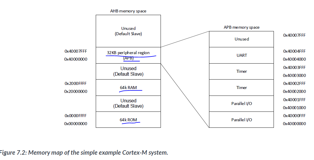
Each peripheral block in this example takes 4kB of memory space. Since the transfer size on the APB is limited to word wize, we can have up to 1024 hardware registers for each peripheral. However, in normal applications, the required number of registers for each peripheral is likely to be far less than that.
The use of 4kB memory size for peripherals is a common practice, which allows us to create a simple APB slave multiplexer which multiplexes responses using bit field of PADDR(e.g.,bit[15:12] for 16 slaves). However, it is fine to use other memory sizes for APB peripherals, although potentially these will requiee a slightly more complex APB slave multiplexer.
->
PADDR의 특정 비트 필드를 사용하여 각 슬레이브에 대한 응답을 선택할 수 있습니다. 예를 들어, 16개의 슬레이브가 있는 경우, PADDR의 bit[15:12]를 사용하여 4비트로 각 슬레이브에 대한 응답을 다중화할 수 있습니다.
For designs using the Cortex-M3 or Cortex M4 processors, in cases where the bit-band feature is to be used, then the allocation of an address in the memory map must avoid conflict with the bit-band alias regions.
7.2 Typical AHB slave design rules
Before we start the design process, it is useful to go through some of the rules in AHB operations.
In this book, we will only cover the rules of AHB slave operations for AHB LITE , and AHB5 as most FPGA designers will only need to develop AHB slave designs and not AHB masters.
- An AHB slave must respond with OKAY without a wait state for IDLE or BUSY: When HTRANS is IDLE(0x0) or BUSY(0x01), HSEL is 1 and HREADY is 1, in ther next clock cycle HREADOUT must be 1 and HRESP must be OKAY(0x0).
HTRANS가 IDLE(0x0) 또는 BUSY(0x01)일 때, HSEL이 1이고 HREADY가 1인 경우:
다음 클록 사이클에서 HREADOUT은 1이어야 합니다.
HRESP는 OKAY(0x0)으로 설정되어야 합니다.-
An AHB slave must respond with OKAY without waitstate if it is not seleted : When HSEL is 0 and HREADY(HREADYIN) us 1, in the next clock cycle HREADYOUT must be 1 and HRESP must be OKAY(0x0)
-
at reset, HREADY output from AHB slaves must be 1(ready), and HRESOP must be OKAY(0x0). This is needed to ensure the AHB system is reset correctly.
-
There should not be any comnibatorial path from inputs of the AHB interface to the output of the AHB interface on an AHB slave. The inputs and outputs must be pipelined(separated by register stage) to prevent combinatorial loops.
-
Error signals on HRESP must be two cycles, with HREADY output(HREADYOUT) low in the first cycle and high in the second cycle. An additional wait state(s) before the error response, but each of the error responses must still contain the two-cycle waveform.
-
Although the HRESP inpu in Cortex-M3 and Cortex-M4 is 2 bit wide, the Cortex-M processors and the AHB infrastructure components that we are designing here do not support RETRY and SPLIT response; SPLIT and RETRY responses are not supported in AHB Lite and AHB5.
-
Ideally, The AHB slave should only be able to insert a limited number of wait states to ensure that it will not lock up the whole system. The common recommendation for the maximum number of wait sates for a transfer is 16cycles- but system designers can increase the limit if necessary. Note that this is only a recommendation. In some cases. it is unavoidable to have longer wait states in AHB transfers if the AHB interconnect components or slave has to deal with data transfer across asynchronous clock domains.
위 설명에 따르면, AHB 슬레이브는 웨이트 상태를 삽입하여 전체 시스템이 잠기지 않도록 해야 합니다. 권장 사항은 한 번의 전송에 대해 최대 16개의 웨이트 상태를 가질 수 있도록 하는 것입니다. 그러나 시스템 설계자는 필요에 따라 이 한계를 늘릴 수 있습니다. 이는 데이터 전송이 비동기 클록 도메인 간에 이루어져야 하는 경우, AHB 인터커넥트 구성 요소나 슬레이브가 더 긴 웨이트 상태를 필요로 하는 상황에서 필요할 수 있습니다.- The minimum memory size of an AHB slave for an ARM system should be 1k bytes. Even if the slave does not need this amount of memory, the remaining memory space should not be used for another AHB slave.
Not only does it reduce the complexity of AHB decoder design, but is can also prevent a burst transfer from going across two AHB slaves, which can cause an AHB protocol violation. The starting addres of the AHB slave should be aligned to its memory size in order to reduce the complexity of the AHB decorder design.
실제로 슬레이브가 필요로 하는 메모리 크기가 1k 바이트보다 작더라도, 남은 메모리 공간은 다른 AHB 슬레이브에 할당되어서는 안 됩니다. 이는 AHB 디코더 설계의 복잡성을 줄일 수 있습니다. 또한, 버스트 전송이 두 개의 AHB 슬레이브를 거치는 경우를 방지하여 AHB 프로토콜 위반을 방지할 수 있습니다.- HEXOKAY can only be asserted in the data phase of an exclusive transfer if there is no error reponse. If a bus slave does not support exclusive transfer, HEXOKAY can be tied low.
With these AHB rules defined, most AHB slaves can be designed with a simple pipeline logic block, as shown here:
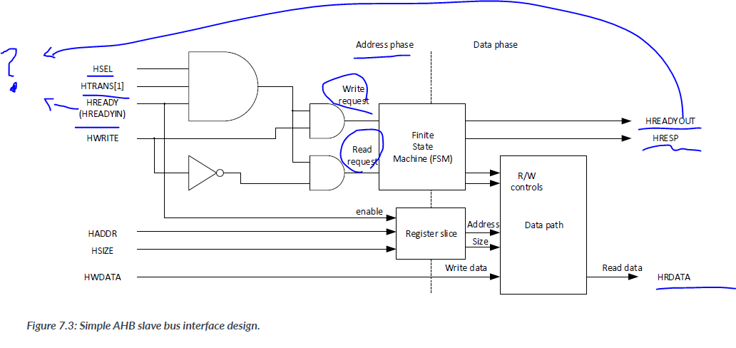
In simpleset AHB slaves, the Finiste state machine can be implemented as a simple register stage if no wait state is required. if multiple cycles are required, the FSM can be implemented as shown:
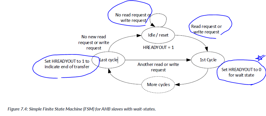
- 1 cycle 에 HREADYOUT가 0 for Wait state
Addtional states will be needed if the device supports error responses on the AHB.
7.3 Typical AHB infrastructure components
After familiarizing ourselves with the AHB slave design rules, we can start looking into the development of the AHB system.
7.3.1 AHB decoders
AHB decoders generate HSEL signals for each AHB slave by decoding the HADDR address signal. The designs of the AHB decoders are system-specific. For the example AMBA system that we are going to develop, the decoders generate the HSEL outputs for the ROM, RAM, APB Bridge, and the default slaves. Two AHB decoders are needed for the example Cortex-M3 system because the AHB bus segment for the I-CODE/D-CODE and the system bus are separated
=> CODE Bus 랑 시스템 Bus 랑 나누기 위해 Decoder 가 두개 필요하다.
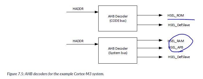
The default slave is an AHB slave that is selected when the address is invalid(i.e., no valid slave is selected). The outputs of the address decoder are comninatorial outputs generated using the address value.
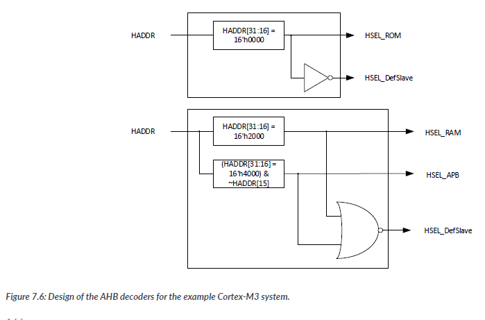
In some situations, an AHB decoder might also take an HSEL input to enable the decode operation if the decoder is only for an AHB subsystem, which is part of a larger AHB system. In the case where an optional HSEL input is implemented, the HSEL outpus would be AND together with the HSEL input, so that the output can only be high if the HSEL input is high. This is required in more complex systems where multiple AHB subsystems are developed, and the address decoder of each AHB subsystem requires a HSEL input from a global address decoder.
7.3.2 Defualt Slave
In an AHB system, if the processor tries to access a memory location that is not assigned or not used, the normal practice is to return an error response to generate a fault exception. This mechanism allows the program to detect that something has gone wrong as an unused address range that should not have been accessed. To generate this response, a very simple AHB slave called the Default Slave is used.
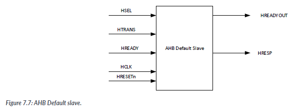
The defulat slave is selected by the AHB adress decoder when an invalid address range is output from the processor. If the default slave is selected and the processor issues an active trasfer(TRANS equals NSEQ or SEQ), then the default slave sends out an error response in the data phase of the transfer.
This behavior is different from most 8-bit or 16-bit microcontrollers. In these products, accesses to an invalid accesses is that the processor can remedy this if an error is detected, and thus increase the robustness of the system.
In some designs the default slave is combined with the AHB slave multiplexer. In this example, we will design it as a separate unit. A simple FSM is used to generate the 2-cycle error response as required by the AHB protocol.
Since we generate an error response for every transfer with invalid accesses, we do not need to worry about the HWRITE control, HSIZE signals, and data values.

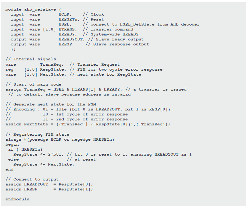
The default slave does not generate any read data and exclusive responses. When connecting the default slave to an AHB system, the unused HRDATA[31:0] signal and HEXOKAY signal(available in AHB5) can be connected to zero.
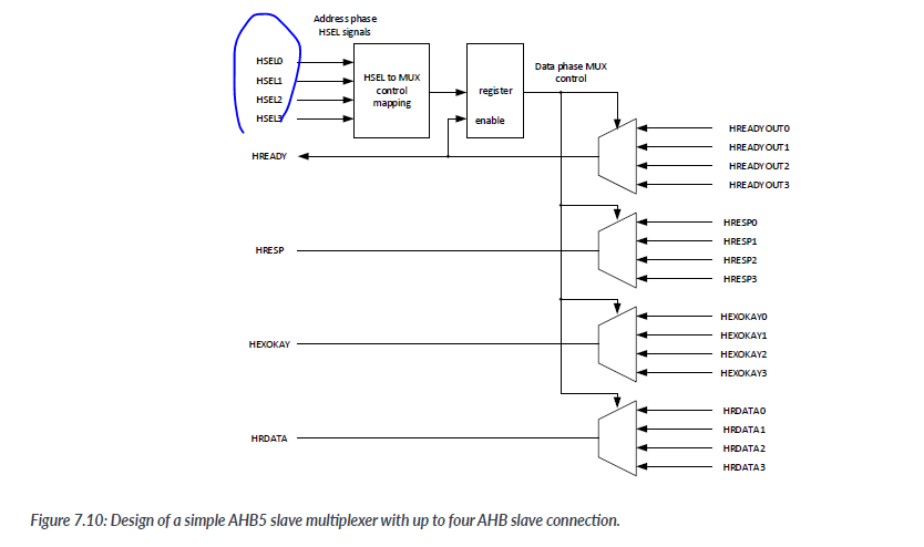
7.3.3. AHB slave multiplexer
The AHB slave multiplexer is needed to connect multiple AHB slaves to an AHB master. In this example, the AHB slave multiplexer connects up to four AHB slaves
7.3.4 ROM and RAM with AHB interface
Please note that, if you are using Cortex-M1 processor, the ROM and RAM are likely to be connected as Tightly Coupled Memories (TCMs) rather than AHB, and the configuration of these memory blocks could be handled by the FPGA design tools.
Two memory models are being developed: a ROM model for program memory and a RAM model is used for program memory, and RAM is used for data memory; however, the RAM model can also be used for program memory if memory initialization is carreid out. In this way, we can allow the program to be self-modified or allow and external debugger to change the program code during debugging.
The ROM model that we have illustrated here is a ready-only simultation memory model. One of the requiremnets for this prgram memory simulation model is that it must allow us to define the program data inside when the simulation starts.
Inside the Verilog code of the ROM model, we use the Verilog system function "$readmemh" to initialize the program data array with data from a file called "image.dat". This file contains the hexadecimal values of a compiled binary image for the Cortex-M processor.
The RAM model. however, will only initialize the data array to zero values. it is possible to add the "$readmemh" function to initialize the RAM content to other values if it is to be used a program memory.
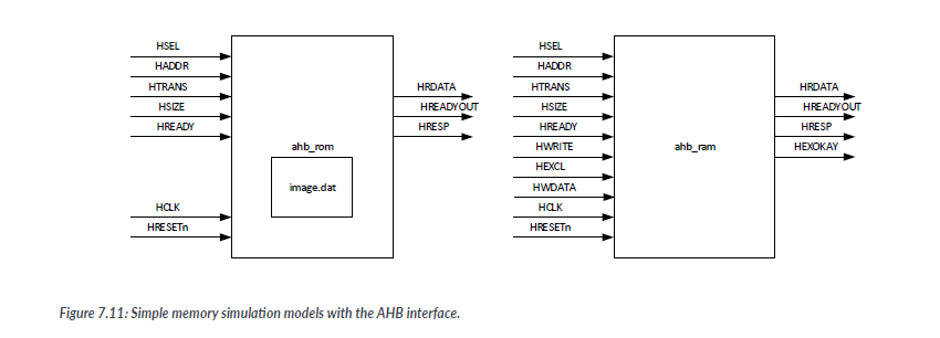
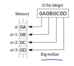
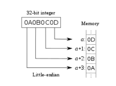
In order to simplify the design, the memory models do not insert a wait state and treat burst transfers just like single transfers. Also, these examplt models only support litte-endian.
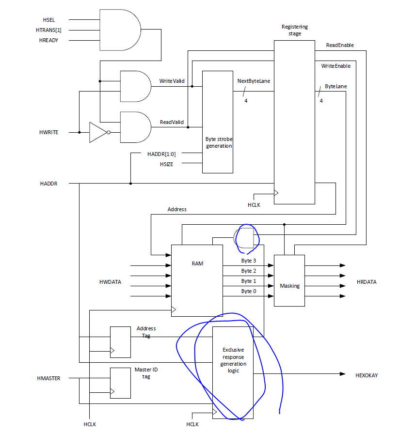
There are different ways to develop the rquired AHB memory simulation models. Since the AHB protocol is pipelined, a registering stage is needed inside the memory. For illustration purposes, we will design the ROM model with a registering stage for the data output, while for the RAM, we will use the registering stage for control signal processing.
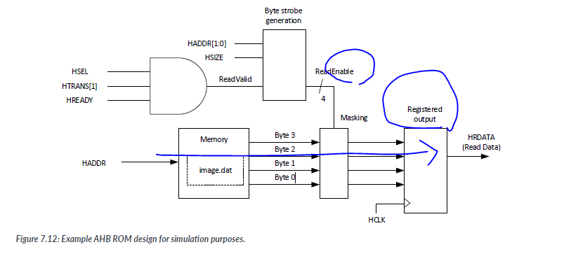
For the ROM design, we assumed that all accesses to the ROM are always read transfers. Therefore the HWRITE signal was not used. In the ROM desgin, we masked the unused read data output for half-word and byte transfer. Note: This is not required in real systems. ARM processors like the Cortex-M3 just ignore the unused data. However, masking the unused data byte can make the bus activities easier to see during debugging.
ROM 디자인에서는 읽기 전송만 고려하고 있기 때문에 HWRITE 신호가 사용되지 않습니다. 이는 ROM이 읽기 전용이기 때문입니다. 따라서 HWRITE 신호를 사용하지 않고 읽기 전송만 처리하면 됩니다.

또한, 반워드나 바이트 전송에 대해서는 사용되지 않는 데이터 출력을 마스크 처리했습니다.
Unlike the AHB ROM, the pipleline stage of the AHB RAM design takes place at the time of control signal generation.
All the actual read and write operations take place during the data phase of the AHB transfer. This ensrues that if the data written are read out in the next clock cycle, the updated value will be used for output.
To make it even more interesting, the AHB SRAM example design also adds supports for exclusive accesses by having exclusive reponse generation logic and tag register( for address and bus master ID) for the exclusive access sequecne. Semeaphore dta are normally placed in SRAM, and if another bus master wrties to the same address location during semaphore read-modify-write-operations, the access conflict can be detected by the logic added in this model.
세마포어 데이터가 SRAM에 저장되어 있을 때, 독점 액세스를 사용하는 버스 마스터가 세마포어 데이터를 읽기-수정-쓰기 작업을 수행하는 동안, 다른 버스 마스터가 동일한 주소 위치에 쓰기 작업을 시도하면, 독점 액세스를 감지하기 위해 추가된 로직이 작동합니다. 이로써 액세스 충돌을 감지하고, 동시에 독점 액세스를 통해 세마포어 데이터의 일관성과 안전성을 유지할 수 있습니다.