Handling multiple bus masters
In many microcontroller systems, you can find multiple bus masters such as :
-
Direct Memory Access (DMA) controllers;
-
Peripherals that need high data bandwidth; for example, USB controllers, ethernet interfaces.
In both cases, these units have bus master interfaces to initiate transfers, as well as bus slave interfaces for configuration. To enable multiple bus masters to access the AHB bus system, Arm provides :
-
Simple AHB master multiplexers to support two or three bus masters accessing a single AHB bus segment(shared bandwidth);
-
Configurable AHB Bus Matrix componets(allowing concurrent accesses).
For a simple Cortex-M0 based system with a DMA controller, the system design can look like this.
리눅스에서 DMA(Direct Memory Access)를 사용하여 가상 주소 공간에 데이터를 쓰기 위해서는 다음과 같은 단계를 따를 수 있습니다:

DMA 버퍼 할당: DMA 전송을 위한 버퍼를 할당해야 합니다. 일반적으로 dma_alloc_coherent() 함수를 사용하여 DMA 버퍼를 할당합니다. 이 함수는 커널 내부에서 DMA에 직접 접근할 수 있는 물리적인 주소를 반환합니다.

DMA 설정: DMA 컨트롤러 및 장치를 구성해야 합니다. 이 단계는 DMA 제어 레지스터 설정, DMA 전송 크기 설정, DMA 채널 및 우선 순위 설정 등을 포함할 수 있습니다. 구체적인 설정 방법은 사용하는 DMA 컨트롤러 및 장치에 따라 다릅니다.

DMA 전송: DMA 컨트롤러를 사용하여 데이터를 가상 주소 공간에 씁니다. 이 단계에서 DMA 컨트롤러는 버퍼의 물리적인 주소를 사용하여 가상 주소 공간에 데이터를 쓸 수 있습니다. 일반적으로 memcpy() 함수나 DMA 컨트롤러에서 제공하는 특정 함수를 사용하여 데이터를 복사하거나 전송합니다.

DMA 완료 확인: DMA 전송이 완료되었는지 확인해야 합니다. DMA 컨트롤러는 전송이 완료되었음을 나타내는 인터럽트나 상태 비트를 제공할 수 있습니다. 이를 확인하여 DMA 전송이 완료될 때까지 대기하거나 인터럽트 처리를 수행할 수 있습니다.

DMA 버퍼 해제: DMA 사용이 완료되면 할당한 DMA 버퍼를 해제해야 합니다. dma_free_coherent() 함수를 사용하여 할당한 DMA 버퍼를 해제합니다.

위 단계들은 일반적인 DMA 사용 방법을 설명한 것이며, 실제 사용 시에는 DMA 컨트롤러 및 장치의 제조사 문서와 리눅스 장치 드라이버 관련 문서를 참조하여 구체적인 설정 및 사용 방법을 확인해야 합니다.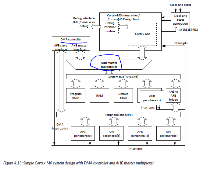
Both the processor and the DMA controller can have a full view of the memory system. The design is simple to create, but the bus bandwidth is shared. As a result , the number of bus masters is supported by the AHB master multiplexer component is often limited to 2 or 3. In such systems, it is common to give the DMA controller higher priority as the processor can access the bus very frequently (due to both instruction - fetched and data accesses).
For systems with higher performance needs, the AHB bus matrix component is generally used. In addition, you would also often need multiple banks of SRAM to enable processor and other bus masters to access different bacnks of SRAM at the same time. Otherwise, the bandwidth of SRAM accesses could become the bottleneck.
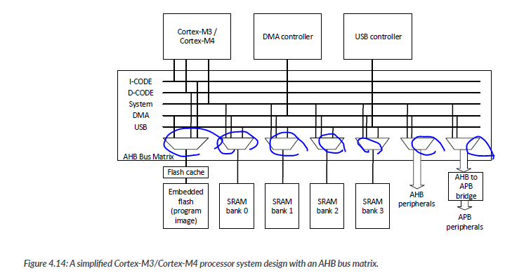
In addtion, to provide higher totoal data bandwidth, having multiple banks of SRAM can also allow some banks of SRAM to be powered dwon when not in use, resulting in lower power consumption in some situations. However, when all banks of SRAM are used, the maximum system power is higher than a signle SRAM bank. Of course, the use of multiple SRAM banks has the advantage of higher data bandwidth, which might mean the overall system-level energy efficiency is still better than one SRAM bank.
AHB bus matrix designs have a concept called sparse connectivity, which means some of the AHB bus master connected to the bus matrix do not need to have access to all of the downstram AHB bus segments.
-
A USB controller doew not need to access to flash program area and peripherals :
-
The I-CODE and D-CODE bus of the Cortex-M3/Cortex-M4 do not need to access SRAM and peripherals because transfer on these buses are linited to the CODE region(unless the SRAM is mapped into CODE region)
The configurable AHB bus matrix Arm supports sparese connectivity, which redueces the bus matrix area and potentially helps to improve timing and speed.
Another supproted feature in Arm's AHB bus matrix is the internal default slave. Since the AHB bus matrix has an internal address decoder to select wich downstream AHB bus segment should be used,it can also detect access to invalid address ranges and route tehm to internal bus matrix, which means that there is no need to add another asystem level defualt slave.
The AHB bus matrix is highly flexible and can bring many advantages to system designs. However, please note that it can also introduce latency cycles when switching a bus segment from one master to another. It is possible to optimize a bus matrix to reduce the chance of unnessary bus arbiter switching by customizeing the logic that defines the deault selected bus of forcing the address of the bus to a specific value when the bus is idle.
When designing systems with multiple bus masters, from a security point of view, it is common to make the configuration interface of th e bus masters(e.g., DMA controllers) privileged access only. Ohterwise, if an unprivileged software componet can program a DMA controller. it can use the DMA controller to access privileged - only memories, which means bypassing the memory protection.
4.7 Exclusive access support
Exclusive accesses are supported in Armv7-M and Armv8-M processors. To support exclusive accesses on multipler processor systems, system deginer should add global exclusive access monitors to the system. The monitors should be placed downstream of the AHB bus matrix or AHB master multiplexer, which will merge transfers from different bus masters. The bus interconnect must also provide HMASTER signals to allow the globla exclusive access monitor to know which bus master the trasfer is generated from.
Exclusive access(독점 액세스)는 ARMv7-M 및 ARMv8-M 프로세서에서 제공되는 메모리 액세스 방법입니다. 독점 액세스는 한 번에 하나의 프로세서만이 특정 메모리 위치에 액세스할 수 있도록 보장합니다. 이는 동시에 여러 프로세서가 동일한 메모리 위치에 액세스하는 것을 방지하여 일관성과 안정성을 보장합니다.
In Figure 4.15, there are two banks of SRAM, and each of them need
- The bus slaves connected to the bus segment can contain semaphore data, and The bus slaves connected to the bus segment can be accessed by more than one bus master that generates access to semaphore data.
Bus segments that only contain general peripherals or flash memories (or ohter types of NVM) do not require an exclusive access monitor as there is no semaphore data in these buses.
In single-processor systems, it is possibe to omit the global exclusive access monitor becuase even with other bus masters present(e.g., DMA controller, USB controller),the software can ensure that these other bus masters do not access the semaphore data. Therefore, normally, globla exclusive access monitors are present only on multi-processor systems.
In single-core systems with Cortex-M3, Cortex-M4 and Cortex-M7 processors, which use proprietary exclusive access handshaking signal (EXREQ and EXRESP), if an AHB bus segment does not have an exclusive access monitor:
Where the bus contains SRAM, tou can tie EXRESP low (do not tie EXRESP high as OS semaphore functions using exclusive accesses will always fail).
Where the bus segment only contains NVM or peripherals that do not semaphore data it is valid to tie EXPRESP high to indicate exclusive access to such address range is not supported.
In single-core system with Cortex-M23, Coretex-M33 and Cortex-M35P processors, which use AHB5 bus protocol with exclusive access support(HEXCL and HEXOKAY):
If the bus contains SRAM, you can use a simple glue logic to assert HEXOKAY in data phases of exclusive accesses ( do not tie HEXOKAY high as AHB5 protocol requires that HEXOKAY is asserted only when HREADY is asserted and must not be high when HRESP is high).
If the bus segment only contains NVM or peripherals which do not contain semaphore data, it is valid to tie HEXOKAY low to indicate exclusive access to such address ranges is not supported.
4.8 Address remap
Address remap is a common system design technique used in Cortex-M microcontroller that needs to support multiple boot stages or multiple-boot modes. For example in a Cortex-M0 design that needs to support a bootloader ( which executes before the program in embedded flash is executed), address remap allows the memory map to place the boot loader ROM into addres 0x00000000 for startup, and then later maps the embedded flash to 0x00000000 for execution for programs in flash.
To use the address remap function, the system design needs to include a program register to control the behavior of the addres decoder.
For the use case, we mentioned, this control register only needs 1-bit to switch between two memory maps. However, some other devies support multiple boot arrangements, and this register might have multiple bits.
A example of an address map design with remap is shown in Figure 4.16 below :
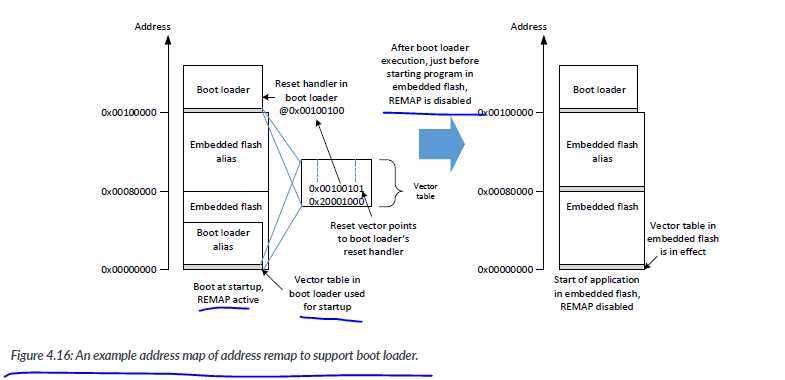
With the arragement shown in Figure 4.16, the vector table in the boot loader is used for booting up the system. The execution of the boot lodar is based on its real address 0x001000000. However, during this period, the vector table in the boot loader alias is still being used. After the bootloader has finished its work. it switches the REMAP off so that the vector table fo the program image in embedded flash is used. it can then read the vector table of the application, set up the MSP value, and branch into the reset handler.
Please note the embedded flash might also have an alias address range to allow the boot loader to handle flash . Otherwise, the beginning of the embedded flash address range will not be visible as the bootloader alias is placed there during start- up
In the design of the remap control register, there are several considerations :
In many system designs, the remap control register needs to be privileged access only for security.
In some systems , it is desirable to make the remap control register reset by power on reset so that the bootloader only excutes once, and does not get executed again during debugging ( the debugger normally resets the target using a system reset, with SYSRESETREQ field in AIRCR).
In some systems, the remap control register could be designed to only be switched off but cannot be switched back on by software. This arragement is used by some secure boot systems where the inofmation associated with the security checks are hidden inside the boot loader and are masked out after REMAP is switched off.
In addition to bootloader use cases, a remap arrangement is also used to allow part of the SRAM to be used as a vector table in systems with Cortex-M0 processors becuase Cortex-M0 does not have a programmable Vector Table offset Resiter(VTOR). In such usage scenarios, a REMAP control register bit is needed and defaults to off(no REMAP). When set to 1, a portion of system SRAM is aliased to the first 192 bytes(maximum vector table size in Cortex-M0) of system memory. Before setting the REMAP control register, software should copy the original vector table to the SRAM that will ten be remapped so that exceptions can still work afterward.
The remap feature is supported by the AHB bus matrix designed by Arm. Howeverm for processors with VTOR, there is no need to us REMAP to allow runtime updates of vec tor tables because you can program VTRO to point to the SRAM area. In newer Cortex-M processor
4.9 AHB-based memor y connection versus TCM
some embedded processor support Tightly-Coupled Memory(TCM). In some cases, the availability of a TCM interface makes memory intergration easier. However, memories like SRAM can also be connected to AHB using AHB SRAM wrapper, such as the one bundled in Cortex-M0/M3 DesignStart.
In terms of performance, at the interface level, TCM and AHB provide the same read access latency. Write access timings are different, but at the processor pipeline level, the write could still be a single-cycle, even when using an AHB interface(e.g., when the processor has a write buffer, or when the AHB pipeline is mapped into two stages of the processor's pipeline).
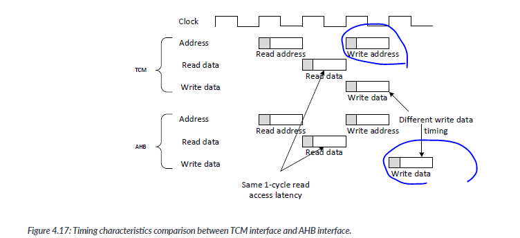
some designers suggest that a dedicated TCM interface could be beneficial if the bus is often occupied by other transactions from other bus masters.
In that situation, access to TCM will not be delayed by other transactions from other bus masters. However, if using a multi layre AHB approach, processor access to memories can still be cariied out immediately providing that the bus slave segment accessed is not being used by another bus master. Even if a processor upports TCM unless its bus interface supports multiple outstanding transfers, it is impossible to start a new data access while the current memory read/write is on-going.
While having TCM reduces the complexity at th e system level interconnect, the merging of read data from the system bus and TCMs is placed inside the processor, so there is no area saving. Potentially, the TCM design might restrict the address range and size of the memories while connecting memories on the AHB instead coulbe more flexible, as designers can sutomize address ranges and memory sizes based on application needs. it is also possible to optimize the AHB bus structure to minimize timing delays between the processor and the memory blocks
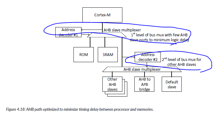
In some processor designs, the use of TCM is required to allow deterministic interrupt resposes. For example, in the Cortex-M7 precessor, access tomemories on the AXI bus system can have non-deterministic timing due to cache hit/miss scenarios. Having TCM enalbes interrupt services to be carried out quickly in deterministic manners. But in small processors like Cortex-M0 to Cortex-M33. the omission of a TCM feature is not a real issue.
4.10 Handling of embedded flash memories
4.10.1 IP requirements
Embedded flash memories are widely used in microcontrollers. They are process node-specific, so if you want to use embedded flash in your design, you need to license it from the foundry of your choice(or their partners that offer embedded flash macros that are compatible with the process node)
In addition to the embedded flash memories, you need an embedded flash memory controller IP taht links the embedded flash to AMBA buses, and potentially system cache IP. The flash memory controller IP can be flash technology-specific; however, in 2018, Arm anoounced the Generic Flash Bus(GFB) standard, making it possible to create generic embedded flash controllers and allow embedded flash macros to be connected to those contorllers via simple glue logic,, which is process technology-specific. Arm aloso offers embedded flash controllers based on GFB interface.
Embedded flash memries are usually quite slow(e.g.,30MHZ to 50MHZ access speed for most of the low-power embedded flahs macros). Typically , caches in some form are needed to enalbe the processor system to run at higher clock psees. Having caches also enalbes better energy efficiency by reducing the memory accesses on the embedded flash(which could be relatively power-hungry).
Such cache components are available from Arm and other IP suppliers. For example, the AHB flash cache is part of Arm Corstone-100 foundation IP.
4.10.2 Flash programing
Normally, embedded flash memories parition the memory space into pages. To update flash memories, the update process has to be done on a page by page basis ; i.e., you cannot update just a few bytes/ words of the flash. the flash programing and erase operations are supported by the embedded flash controllers mentioned errlier. For secuiry reasons, the programming interface of the embedded flash controller should be privileged access only. If TrustZone security extensions are used, then it needs to be restricted to secure privileged access only to enable secure firmware updates.
When doing flash programming, instead of using debug connection to access the flash controller directly, the common approach is to :
Download a small piece of code to SRAM called a flash programming algorithm, and Download a block of data for a flash page to be programmed to SRAM, then Download addtional confuguration information and Set the PC to the flahs programing algorithm, before executing the code to program the flash page.
Each time a flash page is programmed, potionally, the flahs programming algorithm can verify the contents of the page. The debug host can then download another page of data nad repeat the process until all tepages are programmed.
If a device contains TrustZone security extenstions and the on-chip secure firmware is already loadded to the device, the flash programming algorithm might already be present within the on-chip firmware.
In such cases, the flash programming sequence only needs to load the new flash contents and configurations before triggering the flahs programming steop.
4.10.3 Bringing up a new device without a valid program image
One of the common questions from new Cortex-M designers is : How can you bring up a microcontroller device first time without any valid program in the embedded flahs? The achtual Sequenci is no different from normal flash programming :
When the device starts up for the first time, since the flash does not contain a valid program image, it will quickly enter fault exception and eventailly fo into lock up state.
Even if the device is in LOCKUP state, the devugger can still establish a debug connection via JTAG/Serial Wire.
The debugger can then enable a reset vector catch(a debug feature in the Cortex-M processors),and use System Reset Request (by programming Application interrupt and Reset Control Register to reset the system. When the processor comes out from system reset, it enters halt state immediately because ther reset bector catch is enabled.
The debugger can download the flash programming algorithm and pages of program image into SRAM and set the PC to lauch the flassh programming algorithm.
When all the requried flash pages are programmed, it can reset the system again to start the application or to debug it.
The same concept can also be applied to device taht run code from external flash.
