9.1 Creating a simple microcontroller-like system
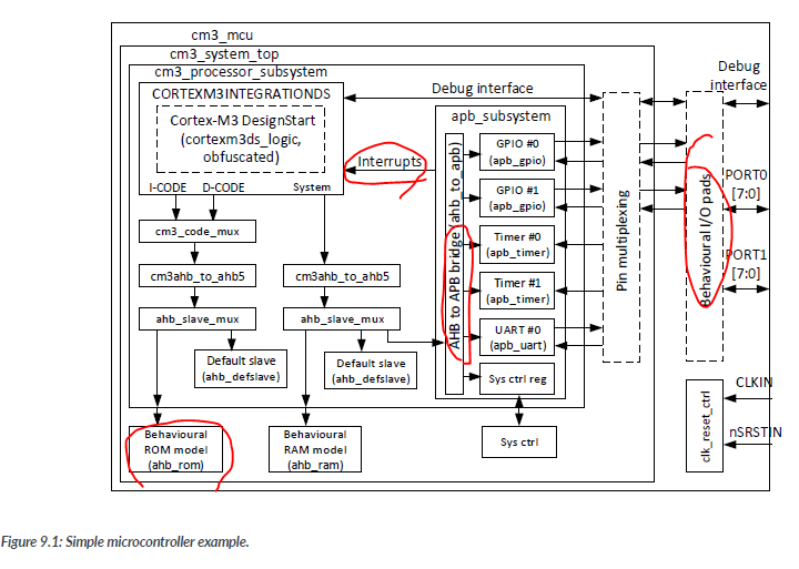
After designing the bus infrastructure components and peripherls, we can then put together a processor system and simulate it in a simulaor. In this section, we will cover a very simple microcontroller-like design based on the Cortex-M3 processor and the components that we created in the last two chapters.

The desing contains multiple levels of design hierarchy - as follows :
The processor subsystem contains the processor and the bus infrastructure components, as well as the APB subsystem where digital peripherals are located.
The APB subsystem contains the AHB to APB brdige, as well as peripherals(digital parts only).
In this example, we have :
- Two GPIO ports(8-bit each);
- two timers;
- One UART;
- Resisters for system control function are also placed here.
- The behavior memory models are one level up in the design hierachy(cm3_system_top). - This level also contains the pin multiplexing.
- The top-level of the microcontroller contains the top-level of the Cortex-M3 system the clock reset control(e.g, clock gating, reset synchronizers) and I/O pads.
This is a simple design just for illustration and educational purposes. In the real world, microcontroller designs are likely to be musch more complex; for example:
- Most commercial microcontrollers have a lot more peripherals, including analog peripherals.
- In real microcontrollers, there might be additional bus masters such as DMA controllers.
-In SoC designm RAM, ROM(or embedded flash macros) would be likely to have power management/ control features.
-If embedded flash is used, flash programming support requires addtional control registers and a voltage booster(e.g., DC-DC converter).
Many microcontrollers also have on-chip DCDC converters to provide lower voltage( ~ 1 to 1.2 volts) for digital circuitries. The supply voltage for the chip normally ranges from 1.8 Volts to 3.6 Volts.
Addtional circuits are need for chip manufacturing testing.
power management in modern microcontrollers can be quite complex. For example, there can be multiple power domains and many clock domains and runtime power mode options. In addition, some of them have separate _retention SRAM _for holding crucial data while in very low-power sleep modes.
-> retention SRAM 도 분리해야된다.
Various security features might be needed depending on targetd applications.
9.2 Design partitioning
After looking at Figure 9.1, some of you might wonder if there is anything that needs to be considered when defining the design hierarchy? There are indeed several aspects to bear in mind, notably:
-
The cm3_processor_subsystem-level contains only synthesizable components. This enables us to synthesize most of the digital parts in one go.
-
If the memory macros require bus wrappers, we can also move the bus srappers into the processo subsystem in order to synthesize them all in one place.
-
A periheral/APB subsystem is designed as one unit - this allows it to be resued in multiple designs. The system control function is split into two halves : one part of it is in the programmable regiaters inside the APB sub system, while the other half is located at a higher level. The reason is that in many SoC designs, the system control function might involve non-syntehsizeable IP such as voltage control or clock control logic. If a system contains analog peripherals, then it is also possible to use the same arragement to separate synthesizable and non-synthesizable parts of any analog peripherals in the design hierarchy.
Pin multiplexing is also placed outside of the processor subsystem - this enables the same peripheral subsystem to be used with different projects, which can have different chip package and hence different pin multiplexing
-
I/O pads are instantiated in the design(in this example, behavioral models of I/O pads are used for simulations). In SoC designm it is often essentail to instantiate I/O pads based on electricla characteristics of the pin functions.
-
Usually, various types of input, output, and tristate pads are available for each semiconductor process node with different drive strengths and different speeds. The behavioral models for I/O pads can be used difrectly in FPGA synthesis, as FPGA development tools can help you define I/O characteristics using a project's configuration files.
-
Clock gating is handled at a high level in the design hierarchy. This can help simplify the setup of clock tree syntehsis. in this case, the clock gating is done in a desgin unit called clk_reset_ctrl at the top-level.
-
If your SoC design needs to support multiple power domains, it is also important to partition designs based on the power domains. In design units where multiple blocks of different power domains are present; it is best not to have any logic functions inside those hierarchical files to simplify power domain handling in implementation flow.
-> SoC 설계가 여러 전원 도메인을 지원해야 하는 경우, 전원 도메인에 기반하여 설계를 분할하는 것도 중요합니다
9.3 What is inside a simlutation environment?
A number of Verilog simulators are available onthe market. In the majority of Arm Cortex-M processor deliverables, we support the following products: Mentor Modelsim/Questasim, Cadence NC Veilog, and Synopsys VCS. Other simulators could be used, although the deliverables only include the simulation scripts that are mentined above.
To simulate the simple MCU design, we also need a testbench. A testbench is a simluated environment in which the microcontroller system will be working. In addition to the processor system, which we will call DUT(Device-Under-Test), the simulation environment typically contains a number of other components:
Clock and reset signal generator(s).
Trickbox(es) that provide input stimulus to the DUT and might also interface with outputs from the DUT. This is optional. In the case of testing a microcontroller-like system, it is possible to use some form of loopback signal connections as a trickbox to test peripheral interfaces.
- In some cases, simulation models of external memories or external peripherals might also be needed to test some of the interfaces on the DUT. For example, if your system design supports external memories, then you will need to add a model of the external memory in the testbench for testing external memory accesses.
-
For a processor testbenchm it is also common to add some mechanism to allow message display under the control of software inthe processor.
-
Other verification components - one of the techniques for verification is to add a rang of verification components like bus protocol checkers in the simulation(some of these components can be inside the DUT). If something goes wrong, for example, illegal bus bahavior is obsered, the verificaiton component can stop the simulation and report the errs.
In our example testbench, a UART monitor(uart_mon.v) is used to display text messages generated by software(e.g., using pringt function). This unit is also used to end the simulation when it receives a peicial character.
To run a system-level simulation, the program memory of the processor system also needs to contain a valid program. Therefore, we need to prepare some minimal softwre code and a compliation set up to enable us to do a basic simulation.
9.4 prepare the minimal software support for simulation
9.4.1 Overview of example code based on CMSIS-CORE
| file | description |
|---|---|
| cm3_mcu.h | Device- Specific header based on CMSIS_CORE. This contains the peripheral register definitions and interrupt assignments. |
| startup_cm3_mcu.s | Assembly startup file - this contains the reset handler, efault handlers, and the vector table |
| uart_util.c | Simple UART funcitons to configure the UART and basic UART transmit and receive function. This is used for supporting message idsplay during simulation. |
| system_cm3_mcu.c | This provides Systeminit(void) usually used for system clock initialiation |
| system_cm3_mcu.h | header file that declares function availabie in system_cm3_mcu.c |
| system_cm3_mcu.h | Header file that declares functions available in system_cm3_mcu.c |
| hello.c | Simple hello world message display and demo |
9.4.2 Device header file,
One part of the header is interrupt Number definition.
typedef enum IRQn
{
	NonMaskableInt_IRQn  = -14,
    HardFault_IRQn = -13,
    MemoryManagement_Irqn = -12,
    BusFault_IRQn = -11,
    UsageFault_IRQn = -10,
    SVCall_IRQn = -5,
    DebugMonitor_IRQn = -4,
    PendSV_IRQn = -2,
    SysTick_IRQn = -1,
    GPIO0_IRQn = 0,
    GPIO1_IRQn = 1,
    TIMER0_IRQn = 2,
    TIMER1_IRQn = 3,
    UARTTX0_IRQn = 4,
    UARTRX0_IRQn = 5,


} IRQn_Type;
typedef struct
{
__IO uint32_t CTRL; // Offset L 0x00 Control Register
__IO uint32_t CURRVAL; //Offset 0x004 Current Value Register (R/W)
__IO uint32_t RELOAD; // offset : 0x008 Reload Value Register (R/W)
__IO uint32_t IRQSTATE; // offset : 0x00C Interrupt state register
} CM3MCU_TIMER_TypeDef;
The final part of this file that you need to add is the memory map and peripheral definitions :
#define FLASH_BASE 0x00000000
#define SRAM_BASE 0x20000000
#define PEROPH_BASE 0x40000000


#define
9.4.3 Device startup file for example MCU
- Vector table definition :
- Default handler definition.
; vector table Mapped to address 0 at reset

	AREA RESET, DATA, READYONLY
    EXPORT __Vectors
    EXPORT __Vectors_End
    EXPORT __Vectors_Size


__Vectors	DCD __initial_sp	; Top of stack
			DCD reset_handler ; Reset Handelr
-> EXPORT는 어셈블리어에서 사용되는 지시자(Directive)로, 해당 심볼(Symbol)을 외부로 공개(export)하도록 지정하는 역할을 합니다. 외부에서 해당 심볼에 접근하고 사용할 수 있도록 합니다.
9.5 System-level simluation
9.5.1 Compiling hello world.
# Makefile using Arm compiler

# Makefile using Arm Compiler 5

# Include 디렉토리 경로 설정
INC_DIR1 = cmsis_include
INC_DIR2 = .

# 사용자 정의 매크로 설정
USER_DEF =

# Arm Compiler 옵션 설정
ARM_CC_OPTS = --cpu Cortex-M3 -c -O3 -g -Otime -I $(INC_DIR1) -I $(INC_DIR2)
ARM_ASM_OPTS = --cpu Cortex-M3 -g
ARM_LINK_OPTS = “--keep=startup_cm3_mcu.o(RESET)” “--first=startup_cm3_mcu.o(RESET)” \
--rw_base 0x20000000 --ro_base 0x00000000 --map

# 빌드 대상 및 의존 파일 설정
all: hello.hex hello.lst

# 소스 파일을 컴파일하여 object 파일 생성
hello.o: hello.c
    armcc $(ARM_CC_OPTS) $< -o $@

system_cm3_mcu.o: system_cm3_mcu.c
    armcc $(ARM_CC_OPTS) $< -o $@

uart_util.o: uart_util.c
    armcc $(ARM_CC_OPTS) $< -o $@

retarget_io.o: retarget_io.c RTE_Components.h
    armcc $(ARM_CC_OPTS) $< -o $@

startup_cm3_mcu.o: startup_cm3_mcu.s
    armasm $(ARM_ASM_OPTS) $< -o $@

# Object 파일들을 링크하여 실행 파일(.elf) 생성
hello.elf: hello.o system_cm3_mcu.o uart_util.o retarget_io.o startup_cm3_mcu.o
    armlink hello.o system_cm3_mcu.o uart_util.o retarget_io.o startup_cm3_mcu.o $(ARM_LINK_OPTS) -o $@

# 실행 파일을 Intel Hex 포맷(.hex)으로 변환
hello.hex : hello.elf
    fromelf --vhx --8x1 $< --output $@

# 실행 파일을 리스트 파일(.lst)로 변환
hello.lst : hello.elf
    fromelf -c -d -e -s $< --output $@

# 빌드 생성물 삭제
clean:
    rm *.o
    rm *.elf
    rm *.lst
    rm *.hex
9.7 Verification
-
LINT checking
analyze the desin source code -
Formal Verification
needed for component level verifications. you need to define input constraints( 제약) for the DUT and rules for expected outputs. -
Clock Domain Cross(CDC) checks
Many SoC designs contain multiple clcok domains that are asynchronous to each other, and apprioprate synchronization logic should be in place. CDC checks are used to detect missing synchronization logic(e.g, double flip-flop synchronizers). When using a CDC checker, you might need to add a range of constraints to specified exempted cases(e.g., In some cases, a signal going from one clock domain to another can only change when the destination domain;s clock is stopped).
-> 예를 들어, 신호가 한 클록 도메인에서 다른 클록 도메인으로 전환될 때 메타스태빌리티 문제를 완화하기 위해 두 개의 플립플롭 동기화기를 사용하는 것이 일반적입니다.
-> 예를 들어, 어떤 경우에는 신호가 한 클록 도메인에서 다른 클록 도메인으로 전환될 때 목적 도메인의 클록이 정지될 때만 변화할 수 있는 상황이 있을 수 있습니다.
Netlist simluations
After the design is synthesized and has potentially gone through placement and routing flow, it is common to vack annotate the netlist and timing to double-check the design using netlist simulations with a subset of tests used in RTL level simulation. Due to addtional timing details, typically in the form of SDF (standard delay format) files, netlist simulations are much slower than RTL simulations and therefore re-running all verifications on netlist is typically unfeasible.
While static timing analysis can detect timing violations, netlist simulation is still useful to detect missing or errors in timing constraints. Netlist simulation is also needed to verify scan patterns generated by ATPG tools, as scan patterns often contain user-defined setup patterns at the start of the scan test that need to be verified at netlist level.
FPGA prototype
In addition to demonstration purpose, FPGA prototyping is very useful for validating debug connections and related aspects such as pin multiplexing. Since software developers can create applications and execute them on FPGA platforms as in real applications(potentially at a reduced speed), application developers can use FPGA prototypes to develop application-level tetsting and un the test much quicker than in RTL simulations.
Verificaitons for designs with multiple power domains
If a desing contains multiple power domains, addtional verifications are required:
Power-aware simulations - entering of sleep modes and waking up can be simulated, with some of the power domains powered down during sleep
Power intent verification - veification of power intent desciption (e.g., UPF )
Low-oiwer formal Verificaiton - if a logic operation has moved from one power domain to another due to synthesis optimizations, potentially his can cause incorrect behavior during power down.
Low power equivalent checking can identify such mismatch in behavior.
9.8 ASIC implementation flow

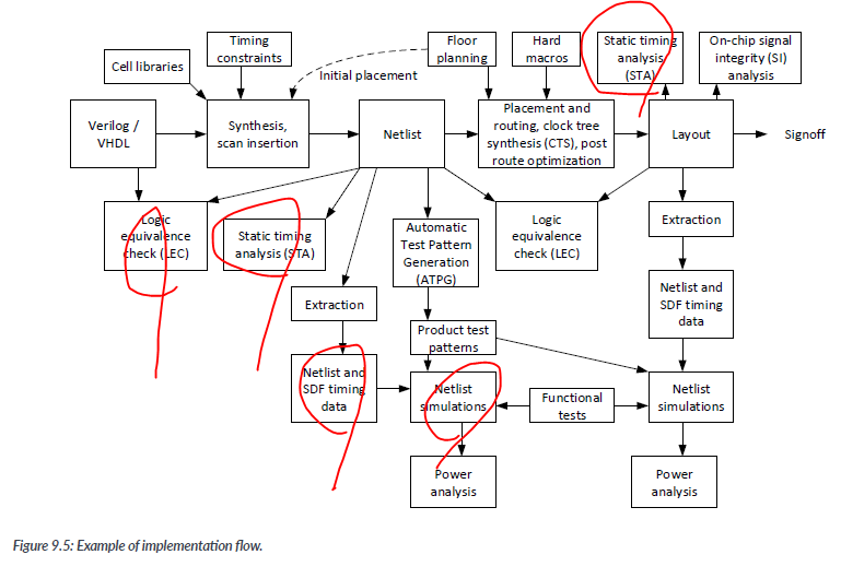
Brief descriptions of some of the key steps in the implementation flow are explained blow.
Some of the checking(STA) might be carried out multiple times during the implementation flow.
Syntesis - Conversion of RTL to netlist. In addtion to the RTL, ASIC synthesis tools also need the cell library and various timing constraints for the clock, reset, and interface signals. Syntehsis processes might include automatic clock gate generation to help low power optimization.
Scan insertion - adding of scan chains to the netlist for chip manufacturing testing.
Static timing anlaysis (STA) - STA tools calculate the timing of the netlist based on timing models of the cell library and check if the design can meet the timing constraint requrie ments. The analysis involves multiple "corners" to detect potential failures like setup timing violation(circuit running too slow) and hold time violation (a signal changes so fast that a register capturing it can end up with an incorrect value).
Placement and routing - The tool places the logic gates in the chip layout and connects the signals between logic gates. Potentially, the placement can be divided into two stages : initial placement provides a rough location of logic gates to enable better iming optimizations during synthesis, and then a second stage finalizes the locations of the gates.
Clock tree synthesis(CTS_ = CTS inserts clock tree buffers to ensure that clock signals reach the different registers at the right time. In a SoC design, two registers receiving the same clock signal might see the clock edge at different times if they are not in the same area on the chip(due to the propagation delay of the clock signal). CTS can balance the clock tree accordingly so that signal paths between the registers wstill work after placement.
-> SoC 설계에서 동일한 클록 신호를 받는 두 개의 레지스터는 칩 상의 동일한 위치에 있지 않을 경우 (클록 신호의 전파 지연 때문에) 클록 엣지를 다른 시간에 볼 수 있습니다. CTS는 클록 트리를 균형 있게 조정하여 레지스터 간의 신호 경로가 배치 후에도 작동하도록 합니다.
Logic equivalence checking(LEC)- this ensures that the functionality of the design units matches the RTL code. If the LEC check fails, the reason could be an error in the design, missing constraints in the synthesis or LEC setip, or potentially something has gone wrong in the synthesis.
-> LEC는 설계 유닛의 기능이 RTL 코드와 일치하는지 확인합니다. LEC 체크가 실패하면 설계 오류, 합성이나 LEC 설정에서 누락된 제약 조건, 또는 합성 중에 문제가 발생한 것일 수 있습니다.
Automatic Test Pattern Generation(ATPG) - ATPG analyzes the netlist and generates scan patterns for chip manufacturing testing. ( There can be multiple types of scan patterns for different test purposes).
-> ATPG는 넷리스트를 분석하고 칩 제조 테스트를 위해 스캔 패턴을 생성합니다. (다양한 테스트 목적에 따라 다른 유형의 스캔 패턴이 있을 수 있습니다).
On-chip signal integrity( SI ) analysis - This can help prevent chip failures caused by cross-talk betwwen wires, and static and dynamic voltage drops in power rails during circuit activities.
-> 이는 전선 간 크로스토크, 회로 활동 중 전원 레일의 정적 및 동적 전압 강하 (IR 드롭)에 의한 칩 장애를 방지하는 데 도움이 됩니다.
Power analysis - this enables designers to confirm that the chip can operate within the power budget.
-> 이를 통해 설계자는 칩이 전력 예산 내에서 작동할 수 있는지 확인할 수 있습니다.
There can be addtional steps required, for example, when dealing with embedded memory macros. Designers need to use memory compilers to generate the memory macros.
-> 내장된 메모리 매크로와 관련된 추가 단계가 필요할 수도 있습니다. 설계자는 메모리 컴파일러를 사용하여 메모리 매크로를 생성해야 합니다.
9.9 Desing for Testing/ Testability
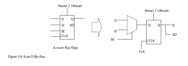
This is one of the most common approaches used to today for testing of digital circuitries. To use sacn tests, the filp-flops in the circuit design in clude additional ports for sacn test operations :

The extra signals on the scan D flip-flop include :
SI - scan in ;
SO - scan out;
SE - scan enable.
After synthesis with scan enalbe(i.e., sace registers are used), we can then create sacn chains using scan insertion in systhesis tools. There can be multiple scan chains in a design(but not too many, as there are restrictions in the chip testers), and the more scan chains you have, the shorter each chain would be and can shorten the time required for running scan tests.
With the scan chain in place, we can then use a tester hardware call Automatic Test Equipment(ATE) to shift in any test patterns to the logic by applying a series of clock pulses with scan enable asserted, and clocked the design with scan enable de-asserted to exercise the functional logic(capture cycle).
During a scan test , it is often essential to bypass internal clock gating and internal reset generation circuits to allow ATE to have direct control of the clock and reset. Therefore, in Arm IP designs, you might see signals like this;
CGYPASS - clock gating bypass;
RSTBYPASS - internal reset generation bypass;
SCANMODE - Scan mode indication / control to force components to work in certain ways to help test coverage. For example, wrappers of memory macros can route write data to read data so that data paths can be tested easily.
These signals should be high during the whole duration of the scan test, including capture cycles.
In some cases, a setup pattern needs to be added to the beginning of thest patterns t o enable scan tests. For example, the scan test pins might be multiplexed with other function pins and need a special signal sequece to enable the scan pin access. Such a setup pattern is defined by the chip designers.
The ATPG tool can generate different types of test patterns. The typical scan test is targeted at detecting stuck-at faults, which means that is checks the inpus and outputs of logic gates are not stuck with a calue of 0 or 1. it is also possible to generate scan test patterns for IDDQ(Idd quiescent) testing, which detects unpected supply current when a certain logic state is reached, which can be an indication of manufacturing fualts/
Scan tests can also be used for at speed testing of some degree. However, in modern ASICs that run at over 100MHz, many ATE might not be able to support at speed testing at such a high clock speed and in those cases, traditional functional tests might be more suiable.
Another tpe of manufacturing test is the memory built in self test(BIST). Memory BIST controllers can be inserted by EDA tools and controlled via JTAG or other test interfaces. When memory BIST is enabled, a memory BIST controller automaticlly creates test patterns to access the memory macros to verify their functions. There can be more than one memory BIST in a chip when there is more than on memory block. to help the integration of memory BIST, Arm processors with internal SRAM provide memory BIST supports. The exact details are processor-specific, so please refer to processor integraiton manuals for more information.
There are also manufacturing test that focus on electrical characteristics of input and output pins. Common examples of these tests include :
Input threshold voltage(VIL, VIH);
Input leakage current(IIL,IIH);
Output driving voltage(VOL,VOH)(can also ceover output drive current test).
제조 공정 중에는 Arm IP 설계의 적절한 기능과 신뢰성을 보장하기 위해 다양한 유형의 테스트가 수행됩니다. 이러한 테스트에는 스캔 테스트와 내장형 자체 테스트 (BIST) 등이 포함됩니다. 또한 입력 및 출력 핀의 전기적 특성에 대한 테스트도 수행됩니다.

스캔 테스트:

CGYPASS (클록 게이팅 바이패스): 이 신호는 내부 클록 게이팅 회로를 우회하여 ATE가 스캔 테스트 중에 직접 클록을 제어할 수 있게 합니다.
RSTBYPASS (내부 리셋 생성 바이패스): 이 신호는 내부 리셋 생성 회로를 우회하여 ATE가 스캔 테스트 중에 직접 리셋을 제어할 수 있게 합니다.
SCANMODE: 이 신호는 특정한 방식으로 구성 요소의 동작을 지시하거나 제어하여 테스트 커버리지를 개선합니다. 예를 들어, 메모리 매크로의 쓰기 데이터를 읽기 데이터로 라우팅하여 데이터 경로를 쉽게 테스트할 수 있도록 할 수 있습니다.
내장형 자체 테스트 (BIST):

메모리 BIST 컨트롤러는 EDA 도구를 통해 설계에 삽입되며 JTAG 또는 기타 테스트 인터페이스를 통해 제어됩니다. 이들은 메모리 매크로에 대한 테스트 패턴을 자동으로 생성하여 기능을 확인합니다. 여러 메모리 블록이 있는 경우 칩에 여러 메모리 BIST 컨트롤러가 존재할 수 있습니다.
전기적 특성 테스트:

입력 임계 전압 (VIL, VIH): 이러한 테스트는 로직 수준의 신뢰성 있는 해석을 위해 필요한 전압 수준을 측정합니다. 낮은 수준 (VIL) 또는 높은 수준 (VIH)으로 구분됩니다.
입력 누설 전류 (IIL, IIH): 이러한 테스트는 입력 핀이 각각 낮은 레벨 또는 높은 레벨에 있을 때 흐르는 전류를 측정합니다.
출력 구동 전압 (VOL, VOH): 이러한 테스트는 외부 부하를 구동할 때 출력 핀에서 생성되는 전압 수준을 확인합니다. 출력 구동 전류 테스트도 포함될 수 있습니다.
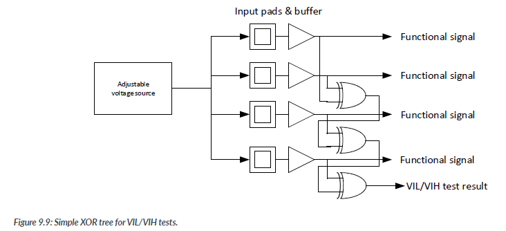
While output pins can be accessed, and their electrical characterisic measured easily, the output signals of inpu pads are inside the ship and creating a test for checking each of the signals can be tricky. To make it easier, we can add a simple logic to link the input pad's outpus together and test them at the same time.

입력 핀들이 모두 동일한 전기적 특성을 가지고 있다고 가정하면, 입력 전압이 유효한 범위 내에 있을 때에도 동일한 출력을 가져야 합니다. XOR 트리에 있는 입력 핀의 개수를 알고 있다면, 예상되는 테스트 결과를 쉽게 결정할 수 있습니다. 입력 전압을 입력 임계 전압 수준에 가깝게 조금씩 조정하면서, 입력 핀 중 하나라도 올바른 신호를 전달하지 못하는 경우 VIL/VIH 테스트 결과 핀이 토글됩니다.
