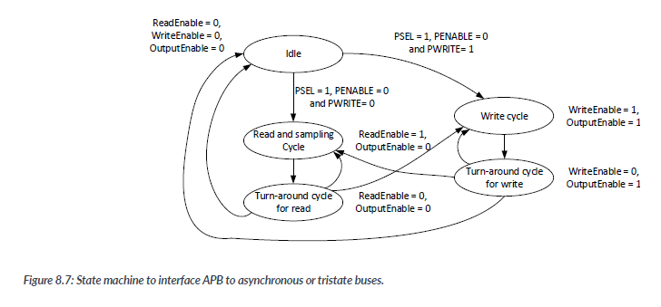
However, if the peripheral requires a tristate bus interface, or uses an asynchronous interface, the wrapper will have to handle the transfers in multiple clock cycles and create a trun-around cycle if a tristate bus is used(a turn-around cycle is used to prevent current spikes on the data bus when the direction of the data changesm caused by the bus master and bus slave tristate buffers being turned on sumulataneously for very short period of time during the transition). In order to allow multiple cycle operations, the APB system must support the PREADY signal, so the APB for AMBA 3 or later is needed in this situation.
The simplest way to develop a wrapper for such a peripheral is to create a finite state machine and generate the read enable, write enable, and tristate buffer output enable, using the state value.( Note : We assume that the OutputEnable signal is used to enable the tristate buffer for write data, and the Read Enable is used to enable the tristate buffer for data output on the slaves). If the peripheral accesses take longer, the finite state machine design can be extended easily by adding extra states.
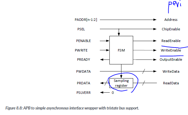
In the example shown in Figure 8.8, a sampling register is used to hold the read data during the trun-around cycle for read. This allows for better synthesis timing performance. Usually, a tristate bus operates slower than a unidirectional bus. Without the samplig regiser, the delay of the read operation, together with the delay caused by the APB slave multiplexer can become a criticla path of the design and limits the maximum clock frequency.
-> Figure 8.8에서 보여지는 예시에서는 샘플링 레지스터가 사용되어 읽기를 위한 턴어라운드 사이클 동안 읽은 데이터를 보관합니다. 이렇게 함으로써 합성 타이밍 성능을 향상시킬 수 있습니다.
8.2.1 General Purpose Input Output(GPIO) interface
In Arm terminology, peripherals that handle a parallelI/O interface are often called General Purpose I/O(GPIO). Some of the commercial I/O interface blocks might be able to support a large number of features, but in here, we are focusing on the APB interface itself, so the design will only provide basic features.
the first stage of the design process is to determine the interface signals required. For basic functionality, we need to have input signals, output signals, and enable control signals for output tristate buffers. We can make the design mor flexible by setting the width of the I/O as a Verilog parameter, with a default width of 8-bot. In this way, the block can be resuesd easily on other designs that need a different I/O width.

The GPIO block will also allow the generation of interrupts to a processor core. In order to make the design more flexible, for each I/O pin, we will provide an interrupt output, as well as a combined interrupt output.
The APB interface will include APB signals for AMBA 3. However, as the design does not require wait state, the PREADY output will be tied to high and PSLVERR signal will be teid to low.
The next step of the design process is to determine the programmer's model for the GPIO block. the prgrammer's model is fairly simple, containing only six registers.
| Address offset | Name | Type | Reset Value | Description |
|---|---|---|---|---|
| 0x000 | Datain | RO | - | Read back value of the IO port |
| 0x004 | Dataoutput | R/W | 0x00 | Output data value |
| 0x008 | OutEnable | R/W | 0x00 | Output Enable(Tri-state buffer enable) |
| 0x00C | IntEnable | R/W | 0x00 | Interrupt Enable(for each bit, set to 1 to enable interrupt generation, or clear to 0 for level trigger interrult |
| 0x014 | IntPolarity | R/W | 0x00 | Interrupt Plarity(for each bit, clear to 0 for rising edge trigger or high-level trigger, and set to 1 for falling edge trigger or low-level trigger) |
| 0x018 | INSTATE | R/W | 0x00 | bit[7:0] - interrupt status, write 1 to clear |
With these details in place, we can begin to develop the design for the example GPIO block.
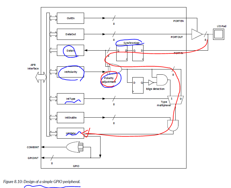
Data in 의 값도 잡고, Interrupt 도 채고.
The GPIO design itself does not contain the tristate buffers. These have to be added externally becuase tristate buffers can be technology-specific, and designers might want to define them manually to match the electrical characteristics needed by the applications. Additionally, in some designs, the I/O pins might need to be shared with other peripherals. In such cases, the tristate buffers would have to be added after the pin multiplexor stage.
The design also contains a dual filp-flop synchronizer. This is used to prevent mestastbility issues caused by toggling of asynchronous external input. The interrupt generation circuit is connected to the synchronizer output. Plase note that, with this arrangement, the interrupt generation will not work if the clock is stopped.
For interrupt generation on the Cortex-M processors with this GPIO unit, Please note that, aside from enabling the interrupt enable at the GPIO block, it is also necessary to program the interrupt enable register in the NVIC in the Cortex-M processor.
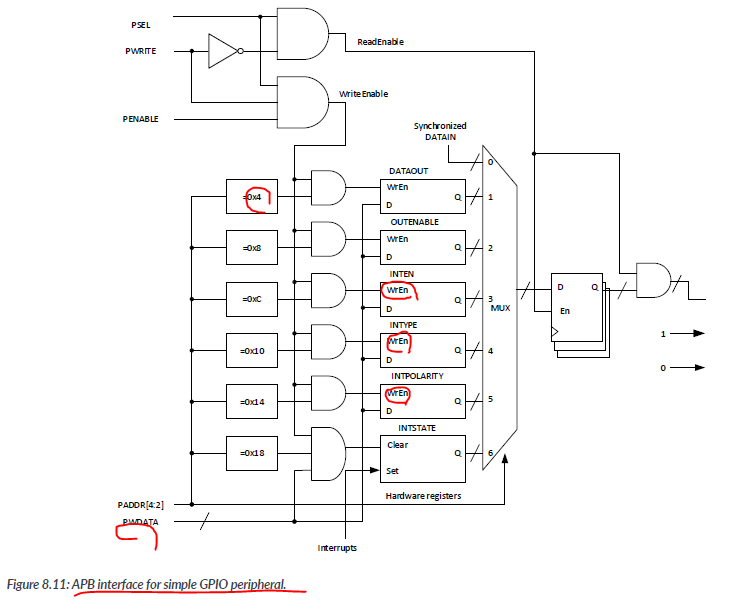
The APB interface design for the example GPIO block is quite simple. First, we use PSEL, PWRITE, and PENABLE to create the enalble signals for read and write operations. Then, we combine these signals with the output from address decoding logic to enable write control for each register and to control the read multiplexer for the generation of read data.
8.2.2. Simple APB Timer
Using a similar approach for the peripheral design, we can also include a simple timer. Unlike the SYSTICK timer, this timer will be based on a 32-bit down counter and has an external input allowing pulse width measurement. The timer can also generate an interrupt when the counter value changes from 1 to 0, and it will automatically reload with a programmable reload value. To make the timer more flexible, we also include an extternal input signal, which can be used as an external enalbe control or as an external clock. This allows the timer to be used for a pulse width measurement of frequency meter. The only other inferface on this timer block will be the APB interface.
The next step of the design process is to determine the programmer's model for the timer block, which is fairly simple as it contains only four registers.
| Address offset | Name | Type | Reset Value | Descriptions |
|---|---|---|---|---|
| 0x000 | CTRL | R/W | 0x00 | Control Register [3] IntrEn-interrupt output enable [2] ExtCLKSel - External Clock Select [1] - External Enable Select [0] Enable - Counter Enable |
| 0x004 | CurrVal | R/W | 0x00 | Current Value |
| 0x008 | Reload | R/W | 0x00 | Reload value |
| 0x00C | INTSTATE | R/W | 0x00 | Bit 0 - interrupt satus, write 1 to clear |
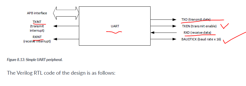
8.2.3 Simple UART
A simple UART is also included in the example test bench. Since this chapter focueses on AHB/APB development, we are not going to cover ther details of the UART design here. The UART has an APB interface simliar to the timer and GPIO. It has the following register :
| Address Offset | Name | Type | Description |
|---|---|---|---|
| 0x0 | CTRL | R/W | Control register(bit[3:0]) [3] receive interrupt enable [2] transmit interrupt enalbe [1] Receive enable [0] Transmit enable |
| 0x4 | CTAT | R/W | Status Register(bit[3:0]) [3] Receive overrun error, write 1 to clear [2] Transmit overrun error, write 1 to clear [1] receive buffer full [0] Transmit buffer full |
| 0x08 | TXD | R/W | Write : Transmit data register Read : Transmit buffer full |
| 0x00C | RXD | RO | Received dta reigster (bit[7:0]) |
| 0x10 | BAUDDIV | R/W | Baudrate divier(bit[7:0]) Minimum value is 32 |
| 0x14 | INTSTATE | R/Wc | Interrupt status [1] - Tx interrupt, wrtie 1 to clear [0] - Rx interrupt, write 1 to clear |
This simple UART design supports 8-bit data transfers with 1 start bit, 1 stop bit, and without either hardware flow control or parity support. Despite being less than 500 lines of Verilog code, it containts a built-in baud rate generator, and the design supports 16 times oversampling on the serial input for better reveive reliabiliy. it also supports interrupt for transmit(when wrtie buffer is emptied) and interrupt for receive(when data is received), For simultaion purposes, a UART monitor module is also included in the exampe testbench to capture the transmitted serial data.
8.3 ID registers
Many Arm peripherals and CoreSight debug components contain a range of read-only ID registers at the end if the 4KB memory spaces. These ID values enable debug tools to identify debug components automaticlly. and they allow the software to determin the revision of the design so that it knows what features are available. In some cases, such informasttion is also useful for software to implement a workaround if certain defects in the pripheral design can be overocme by using software measures.
-> 8.3 ID 레지스터
많은 Arm 주변 장치 및 CoreSight 디버그 컴포넌트에는 4KB 메모리 공간의 끝에 일련의 읽기 전용 ID 레지스터가 포함되어 있습니다.
The ID registers are not strictly required for peripheral operation. In ultra-low-power designs, you can
remove these ID registers to reduce gate count and power consumption.
8.4 Other peripheral design considerations
8.4.1 Security of system control functions
Typically, a peripheral unit that controls the system(e.g., clock and power ontrol functions) should be privileged access only. If TrustZone security is implemented, the functions could also be Secure access only, and Secure Firmware needs to provide APIs for Non-secure software to request system control configuartion updates. This prevents untrusted software from stopping critical system functions.
일반적으로 시스템을 제어하는 주변 장치 유닛(예: 클럭 및 전원 제어 기능)은 특권 액세스만을 허용해야 합니다. TrustZone 보안이 구현된 경우(Cortex-M23 및 Cortex-M33 프로세서의 경우), 이러한 기능은 Secure 액세스만 허용되어야 하며, Secure 펌웨어는 Non-secure 소프트웨어가 시스템 제어 구성 업데이트를 요청할 수 있는 API를 제공해야 합니다.8.4.2 Processor's halting
Potential some peripherals like watchdog timers might need to suspend their operations when the processor is halted. Otherwise, a reset could be triggered unexpectedly during debugging. Some timers(e.g., SysTick timers inside the Cortex-M processors) also stop counting automatically when the processor is halted to allow single-stepping of application code.
->
워치독 타이머와 같은 몇 가지 주변 장치는 프로세서가 정지될 때 작동을 일시 중지해야 할 수 있습니다. 그렇지 않으면 디버깅 중에 예기치 않게 리셋이 트리거될 수 있습니다. 일부 타이머(예: Cortex-M 프로세서 내부의 SysTick 타이머)는 또한 프로세서가 정지될 때 자동으로 카운트를 중지하여 응용 프로그램 코드의 단계별 실행을 허용합니다.
8.4.3 Handling of 64-bit data
In some cases, tiemrs might need to handle 64-bit count values, but the bus interface of a peripheral might be only 32-bit. In such cases, the timer needs to include:
- Include a 64 bit sampling register to allow a 64-bit counter value to be sampled in one go, and then read out using two accesses;
Include a 64bit transfer register to allow a 64bit counter value to be sampled in one go, and then read out using two accesses;
Include a 64-bit transfer register to allow new 64-bit values to be set up using multiple accesses, and then be transferred into the counter using a separted control register.
