4.1 Introduction to the basics of bus design
In this chapter, we will look into the basics of bus system.
there are several generla principles to be aware of :
For processors that support the Harvard bus arhitecture, design the bus system to enalbe concurrent instruction and data access.
Use default slaves to detect access to invalid addresses - this enables bus error to be triggered, and software to handle it when something has gone wrong.
In most of the earilier Cortex -M processor designs, the initial address for vector tables is fixed in address 0x000000. Therefore, the program image needs to be visible in this address at startup.
Minimize the number of wait sates in the memories - in processors that don't have caches, having wait states in the memory system directly impacts the performance, energy efficency, and interrupt latency. In general, wait states in peripheral accesses are less of a problem as those accesses happen less frequently.
Try to keep to a minimum the number of bus slaves on the main system bus.
Seperating the peripheral bus from the system bus has a number of advantages:
A high number of bus slaves in the main system vus could reduce the maximum clock frequency and can also increase the area and power of the bus interconnect. By separating peripheral connections in different buses, address decoding and bus switching logic on the system bus can be optimized for speed becuase most peripherals are grouped as one item vis the bus bridge.
By using a bus bridge to separate the peripheral bus from the system bus, it is possible to provide timing isolation between the two bus segments. This allows the peripherals to be operated at different colck speeds, as well as providing a better chance to get a higher maximum clock frequency on the system bus.
Bus protocol for the peripheral bus is simpler. This reduces the time for peripheral development and testing, as well as reducing complexity and gate counts.
4.2 Building a simple Cortex-M0 system
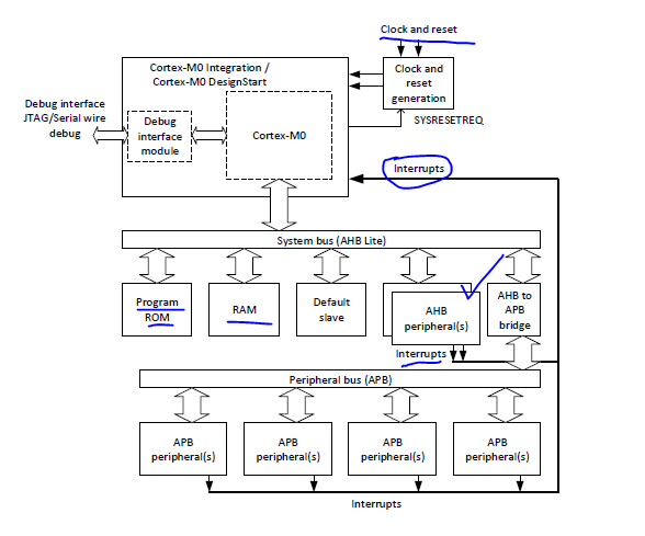
The Cortex-M0 processor is one of the easiest to use Arm processors as it only has one AHB interface for the whole memory system. Typically, a simple Cortex-M0 system design could look like this:
In this example design, ...
The "ROM" (could be embedded flash, or other NVM for holding program image) is placed in address 0x000000 as the initial vector table address is fixed to this location. For FPGA designs, you can use on-chip SRAM with the initial image. Ideally, use zero wait state for "ROM".
The RAM is normally synchronous static RAM with zero wait state to provide the best performance. Usually , we put the RAM in adress 0x20000000, the starting address of the SRAM region.
Some of the peripherals can be designed with an AHB interface to lower access latency(e.g. , GPIO could be designed as an AHB peripheral as some control applications can be I/O intensive).
General peripherals that do not need fast access can be designed with an APB interface and connected via an AHB to APB bridge. Potentially, the peripheral bus can run at a lower clock frequency.
The address ranges of AHB and APB peripherals are usually within 0x40000000 to 0x5FFFFFFF.
The exact arrangement is up to the system designers.
The default slave is selected when the AHB transaction is targeting an invalid address.
For minimum requirements, the top-level of the FPGA/SoC desgin only needs to expose the clock and reset connections, the peripheral interface, and the debug connection.
4.3 Building a simple Cortex-M0+ system
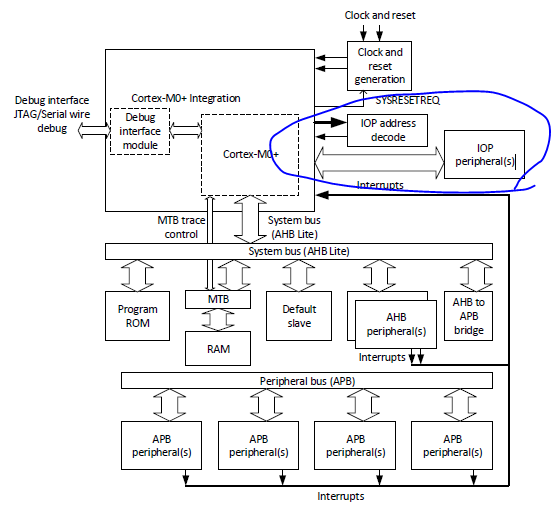
The design of a simple Cortex-M0_system(figure 4.2) can be very similar to the Cortex-M. However, there can be two major differences:
-
Optional single-cycle I/O port(IOP) interface for low latnecy peripheral register access;
-
Optional Micro Trace Buffer(MTB).
If a designer devided to use the single-cycle I/O port interface for a peipheral:
The peripheral might need to use the signle-cycle I/O poert interface for a pehipheral:
The system would need to include a simple IOP address decoder to tell the processor which address range should route to the IOP and which should not. This decoder contains simple combinatorial log ic that decodeds the 32-bit address value, and feedback to the processor that the address belongs to either the IOP or AHB interface.
The MTB feature is used to provide a low-cost instruction trace solution.
The MTB is placed between the AHB and SRAM, working as an AHB to SRAM bridge in normal operations. When used for insruction trace, the debugger programs the MTB to allocate a small portion of the SRAM fro storing instruction trace information. The MTB has a trace interface to receive instruction trace information from the processor and can also generate a debug event (halting request) to the processor.
Typically, the MTB would be configured in circular buffer mode, so that only the recent historty is kept. while it doesn't provide the full software execution history, it is still a useful feature in debugging software issues like providing program flow details just before fault exceptions.
The 32-bit SRAM interface can work with most synchronous on-chip SRAM and FPGA block RAM.
4.4 Building a simple Cortex-M1 system
If you are using Cortex-M1 FPGA DesignStart, you might not need to study the detailed busarrangements as the FPGA design environment may be able to handle this for you. However, if you are using Cortex-M1 in Verilog RTL source form, or just interested to know more details, then this section could be useful.
In many aspects, the system-level integration for the cortex-M1 systme is similar to the Cortex-M0 system:
-
The processor does not have separation of privileged and unprivileged operations ;
-
There is only one AHB interface.
However, there are also some differences:
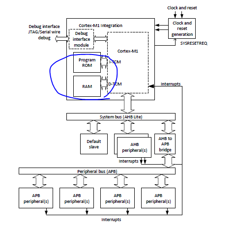
The Cortex-M1 processor supports optional instruction TCM(Tightly Coupled Memory) and Data TCM;
There is no sleep mode support on the current Cortex-M1 processor.
Use of Tightly Coupled Memory(TCM) is common in processor systems implemented in FPGA.
If this option is implemented, the Cortex-M1 processor provides two TCM interfaces,one for instruction memory(I-TCM) and the second one for Data(D-TCM). When TCMs are used, the Cortex-M1 processor can execute a program in its best performance. If excuting a program from memory blocks connected via AHB, the performace/MHz would be lowered because the AHB interface on the Cortex-M1 has an additional pipeline stage to allow it io reach high clock frequency.
TCM can be implemented with RAM blcok inside the FPGA. The details of implementing RAM blocks inside the FPGA depend on the FPGA type and the FPGA design tools you use.
Since the Program "ROM" (it is actually RAMs in the FPGA) and RAM can be connected via the TCM interface, the system AHB connections can be simplified.
-
With debug interface :
-
Without debug interface :
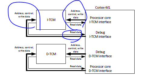
When the debug features are included, the debug interface has a separate set of TCM interfaces(using the block RAM as dual-port RAM).
4.5 Building a simple Cortex-M3/Cortex-M4 system
Unlike the previous simple system descrived in this chapter, the Cortex-M3 and Cortex M4 processors use the Harvard bus architecture and have three AHB interface nad an APB based master interface
| Bus | Types of Transfers | Descriptions |
|---|---|---|
| I-CODE | Instruction fetches and vector fetched for CODE region (0x00000000 to 0x1FFFFFFF) | Read transfers only |
| D-code | Data and devug read/write for CODE region() | |
| System | All Accesses not targeting at CODE region, PPB or internal components (SRAM, Peripheral, RAM Devices, and System/Vendor Specific address range excluding PPB) | |
| Private Peripheral Bus(PPB) | All accesses are in external PPB range(0xE0040000 to 0xE00FFFFF) excluding internal components(e.g., ETM, TPIU, ROM table) | Privileged accesses only |
The multiple bus interface allows instruction fetches and data accesses to take place at the same time (i.e., Harvard bus arhictecture) to get better performance. This requires that the program image and data are on different buses.
In a typical Cortex-M3/M4 system desing :
The program image is placed in the CODE region. Similar to the Cortex-M0 processor, the initial vector table address is fixed at address 0x00000000. Therefore, the ROM(which contains the vector table) needs to visible in this address after a reset.
SRAM and peripherals are connected vis the system bus. Normally in address 0x2000000 and address 0x40000000 ( for peripherals). This arrangement allows software developers to utilize the bit-band feature on SRAM and peripherals.
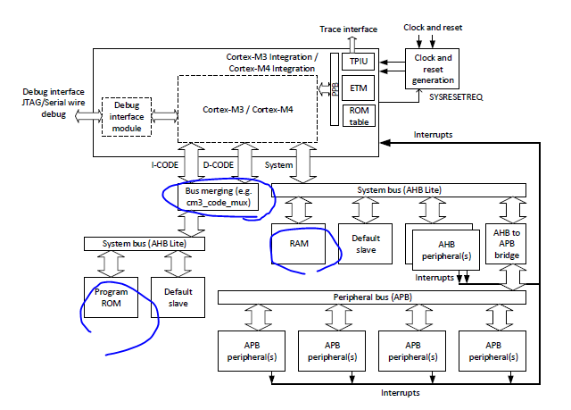
ICODE , DCODE , System BUS 가 다 따로있다.
Since there are two main AHB bus segments, both having some invalid address ranges, we will need default slaves on each of these buses.
The reason for separating I-CODE and D-CODE in the system is to add a literal data cache(on the D-CODE bus) can be read even if the instruction fecth is stalled due to a wait state on flash memory. Typically, flash memories are quite slow(in the range of 30MHz to 50MHz) in comparison to modern microcontrollers, which can run at over 100MHz, When the Cortex-M3 Processor was desfined, a common approach to overcoming flash performance issues was to use flash memories with a wider bus with prefetch buffer so that sequentail instructions could be prefetched while the processor consumed the remaining instructions in the prefetch buffer so that sequentail instructions could be prefetched while the processor consumed the remaining instructions in the prefetch buffer.
Processor's program accesses at 100MHz
However, program operations contain many constant data reads, and these read operations would result in non-sequential accesses, which would be stalled as the dta are not avilable in the buffer. To make matters worse, if the literal access occurred just after the prefetcher started a prfetch, the flash interface needed to wait until the flash read is completed before reading the literla from flash memory. For example, in Figure 4.7 the Processor pipeline needs to stall after the literal data ead until the flash returns the data.
pre fetch 시작 후에 발생하면 플래시 Read 가 완료될때 까지 기다려야함.

해결방법
To help reduce the performance penalty, one solution is to separate the data accesses on a different AHB and put a small literal data cache on it so that literal data used in small loops will not cause latencty after the first loop.
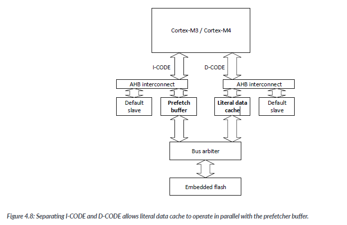
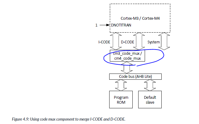
For many simple designs or systems that use system-level caches, there is no need to have such flash access acceleration arrangemnets. System designers can simply merge the I-CODE and D-CODE buses. The Cortex- M3 and Cortex- M4 product bundles provide two components for this purpose:
- Code mux component:
This is a simple bus multiplexer with minimal gate count. To use this component, the DNOTITRANS inpuit of the Cortex-M3/ Cortex-M4 must be set to 1. This prevents the processor I-CODE interface from generating bus transfers at the same time when D-CODE is used.
- Flash mux component :
This component has internal bus arbitration and a register slice to hold I-CODE transfers in a buffer if both I-CODE and D-CODE are active. This can be useful if there are other bus Slaves in the CODE region that could be accessed at the same time as instrcuntion fetches.
In newer microcontroller designs, the use of system-level Cache for embedded flash is increasingly common, Arm provides the AHB flash cache which can be used with various Cortex-M processors with an AHB interface.
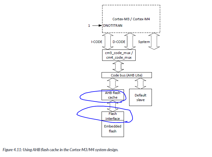
For such systems, the chance for both instruction accesses and literal data having a cache miss is relatively low (except the first time the code sequence is executed of cource), so separating the CODE bus into I-CODE and D-CODE dose not bring a lot of benefits. In newer Cortex-M processors like Cortex-M33 and Cortex-M35P, the I-CODE and D-CODE have been merged to reduce system intergation complixity and to enable lower power.
Instead of having the cache module closely coupling to the processor, the AHB flash cache arragement has the following advantages :
-
The interface between the flash cache and flash interface can be designed as wide bus such as a 128-bit AHB. This enalbes faster data transfers from flash to the cache, and next flash access(e.g., if there is a cache miss) can start earlier.
-
If the code bus has another bus master, the flash cache can provide caching to the other bus master.
Please note :
For Cortex-M3 and Cortex-M4 processors, the internal bus interconnect has a registering stage between the instruction fetch interface and the system bus. Therefore, the performance of the system is reduced if the software image is executed from the system bus.
- Peripheral are expected to be connected via the System AHB(or on a peripheral APB via a bus bridge) instead of the Provate Peripheral Bus(PPB). The PPB intended for debug componets has some limitations; namely;
It is accessible in priviolleged mode only
It is accessibled in little -endian fashion irrespoecive of the processor's data endianness setting:
Accesses behave as Strongly Ordered ( no ohter data memory access can start until the current data access finished);
No bit-band function is available
Unaligned accesses have unpredictable results:
Only 32-bit data accesses are supported
It is accessible from the Debug Port and the local processor, but not from any other agent(processor) in the system.
If needed, it is possible to have an SRAM shared between code and SRAM regions by having bus accesses from both code and system bus(i.e., memory address aliasing). This allows the software to use a signle SRAM block and execute code from SRAM without performance loss :
However, from a security point of view, this needs to be handle carefilly to prevent vulnerabilities. For example, if a memory region is privileged access only, then the access permission needs to be pribileged for both address locations(Alternatively, you can make the RAM visible on only one bus at a time).
