1. Digital System
-
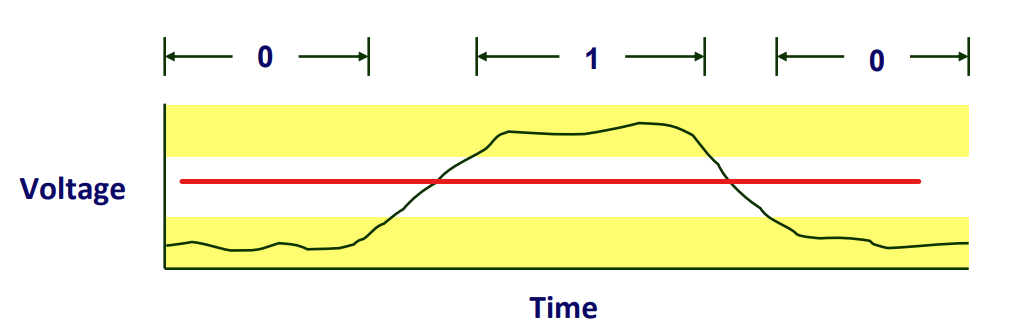
Use voltage to express either high range (1) or low range(0)
-
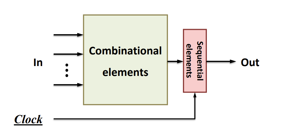
Three components to implement a digital system
- Combinational elements
- Sequential elements
- Clock signals
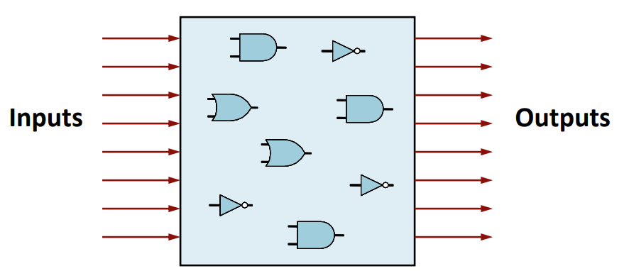
2. Combinational Logic Elements
-
Definition : Input이 결정됨에 따라 output이 자동으로 결정되는 elements
- No embedded state
- Output fully dependents on inputs
- Ex) AND, OR, XOR, NOT, NAND, NOR . . .
-
The examples of combinational elements
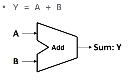
- Adder : 가산기
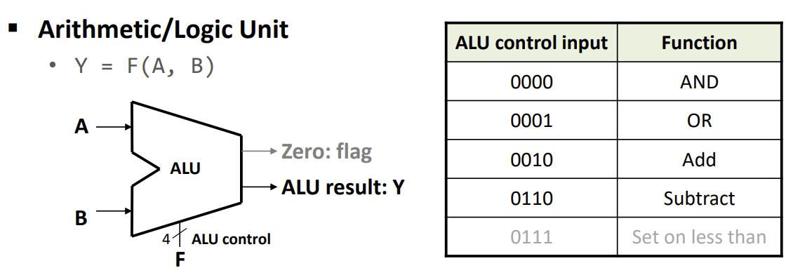
- Arithmetic/Login Unit : 산술 연산
-> ALU result : Y
: 산술 연산의 결과로 ALU control signal에 의해 어떤 연산과정을 가져갈지 결정됨
-> Zero : flag
: BEQ, BNQ와 같이 branch 명령어를 자주 사용하므로 flga의 값 (0, 1)에 따라 빠르게 판단, 연산할 수 있다.
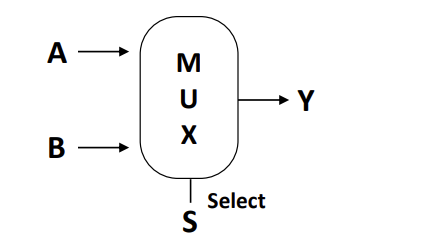
- Multiplexer : Select에 의해서 여러 개의 input 중에서 어떤 값을 선택해서 output으로 사용할지 결정한다.
- Adder : 가산기
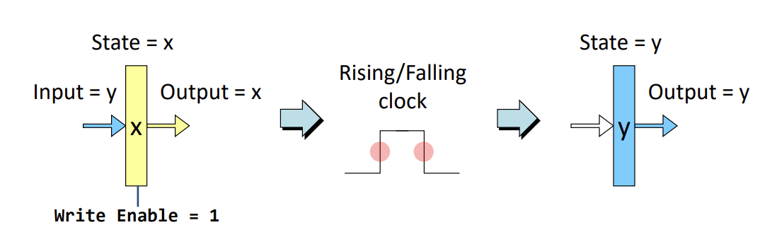
3. Sequential (Storage, State) Element
-
Definition : 현재 State를 가지고 output으로 내보내는 Elements
- Input, Write Enable, Clock signal
-> Write Enable : 1이면 clock edge의 변화 (falling / rising) 를 통해 Element의 state를 바꾸도록 결정
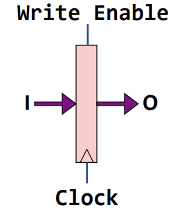
- Input에 따라 Output이 바뀌지 않고 Write Enable 신호로 의사 결정
-> Write Enable 1 : Edge-triggered operation ( Rising / Falling clock)
- Input, Write Enable, Clock signal
-
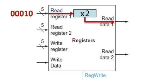
Register File
- Consists of 32 general purpose registers
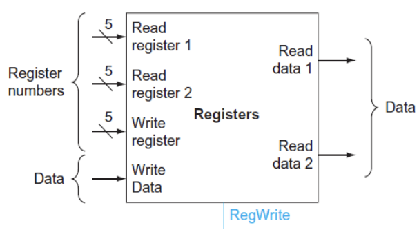
- Input : Read register 1, Read register 2 : 레지스터 읽기
-> Output : Read data 1, Read data 2
- Write register : Destination register 지정 (예 : 5번 register)
- Write Data
- RegWrite (Wrtie Enable)가 1이 되지 않으면 write는 수행 되지만 output은 변하지 않는다.
-> 5번 register를 Read register : 기존 값 그대로 나옴
-> RegWrite 1 → clock edge (falling / rising) → 5번 register를 Read register : Write Data값이 나옴
- Input : Read register 1, Read register 2 : 레지스터 읽기
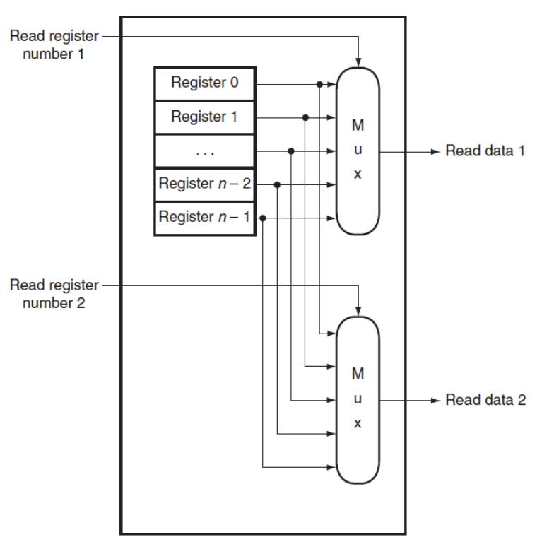
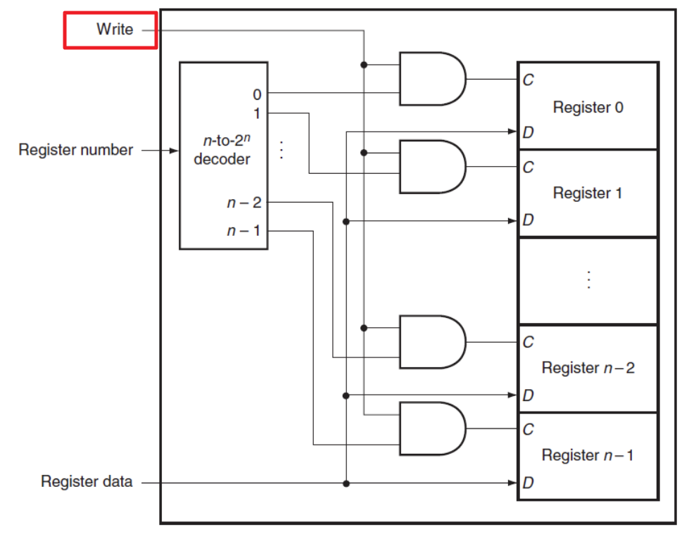
- Register File Timing
- Reading : Output은 input address에 의존
- Writing : clock이 변화할 때 (Rising / Falling) update
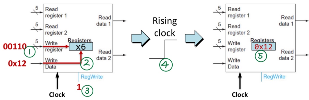
- Reading : Output은 input address에 의존
- Consists of 32 general purpose registers
-
Memory
- has two buses
-> Output bus : Read data
-> Input bus : Write data
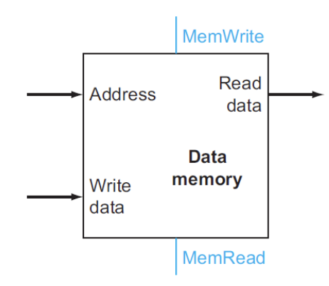
- Address : Target Address
- Read data : target address로 이동해서 데이터를 읽고 data out
-> MemRead : 1 - Write data : target address로 이동해서 Write data를 data in
-> MemWrite : 1 (state를 바꿈) → clock rises/falls → update
-> target address : x1, write data : 0x12 → 레지스터 x1 데이터 값을 0x12로 변경
- has two buses
-
Clocking : Clock cycle ↓ -> frequency ↑ -> Clock cycle time ↓ -> 성능 ↑
- Edge-triggered clocking : falling edge / rising edge에서 상태변화가 일어난다.
- Single cycle implementation : 하나의 cycle에 하나의 instruction이 모두 수행되야한다.
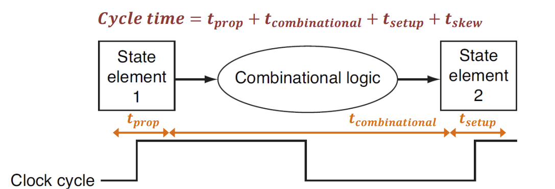
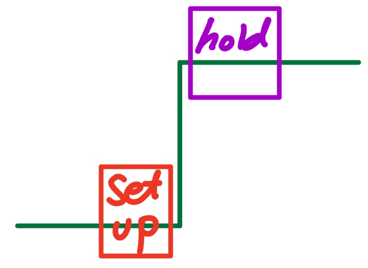
- Cycle time : state element 1의 데이터가 state element 2의 input으로 가서 state를 바꿀때까지 걸리는 시간
- Cycle time = propagation + combinational + setup + skew- Combinational logic : 연산, cycle time을 결정하는 가장 큰 요소
- skew : 모든 Combinational Logic 연산 시간 동일 하지 않음 → 가장 느린 연산을 기준으로 차이를 보상해줌
- setup : edge발생 전에 input data를 유지 해야하는 시간
- hold : edge발생 후에 inpuit data를 유지 해야하는 시간
- propagation : Output data를 확인하려면 edge 발생 후에 일정 propagation 시간이 지나고 나서야 확인이 가능하다.
-> propagation time이 hold time보다 길어서 큰 값이 prop을 cycle time에 포함한다.
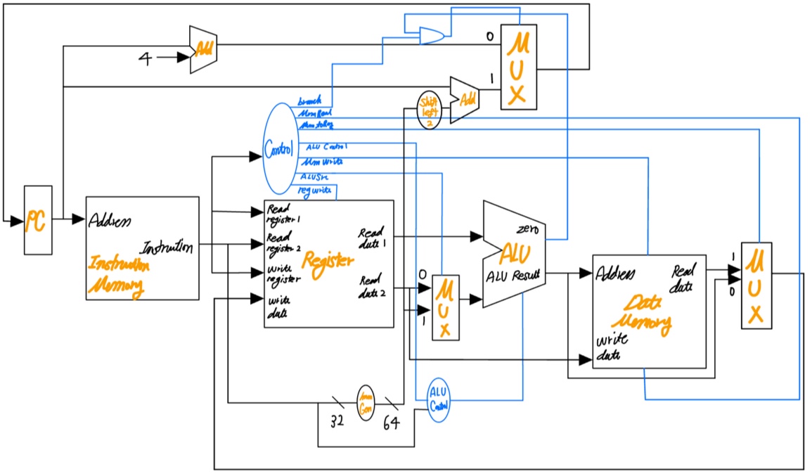
4. Building Datapath
-
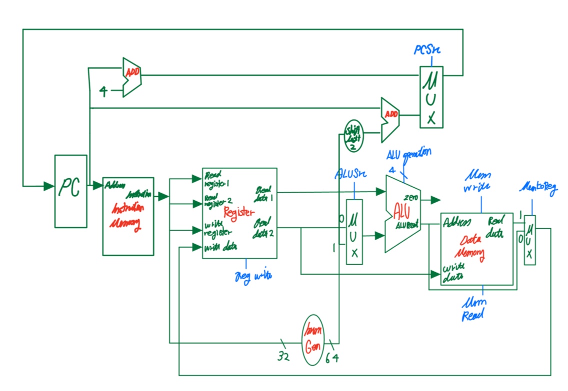
Instruction Fetch : 명령어 불러오기
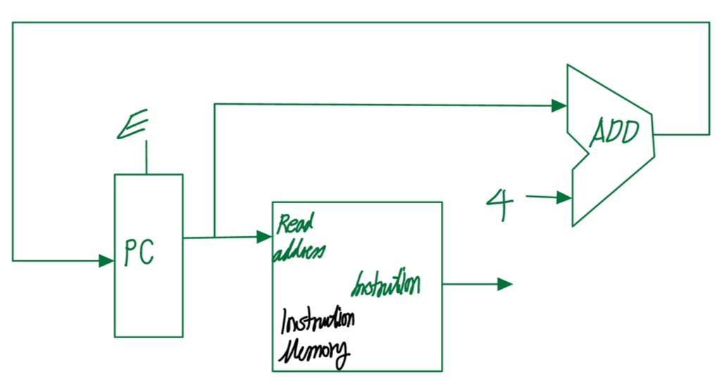
- PC에 담긴 next instruction의 주소를 읽고 instruction을 output으로 내보낸다.
- pc = pc + 4
-
R-Format instructions
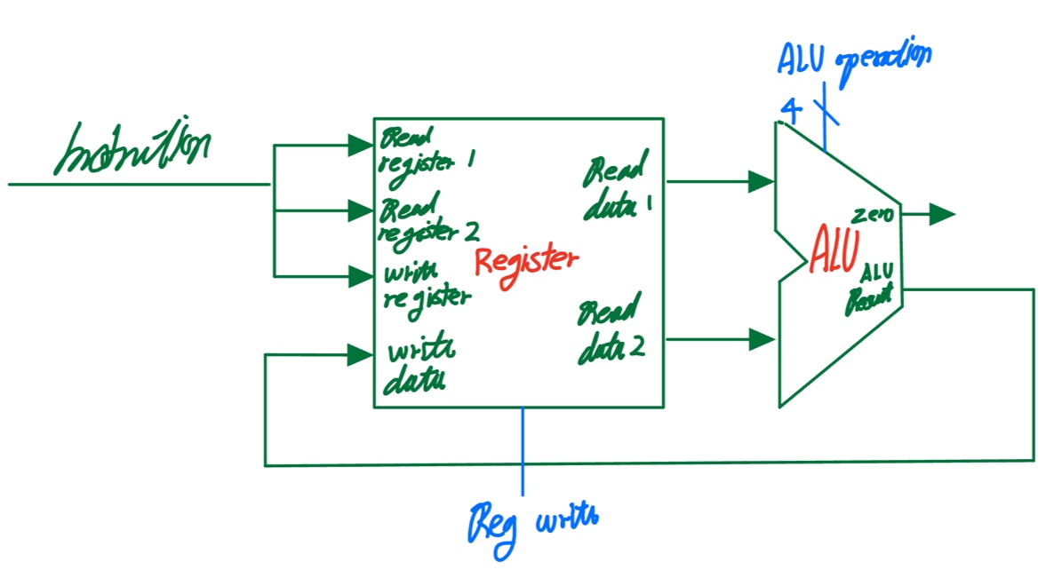
- Ex) add rd, rs1, rs2
- Read data1 : rs1값
- Read data2 : rs2값
- ALU Result (write data) : rs1 + rs2 값
-> ALU operation은 4비트로 16가지의 서로 다른 연산을 가질 수 있으며 Instruction의 opcode에 의해서 결정된다. - Reg write 신호가 1로 바뀌면서 clock edge 발생 → rd값에 write data가 쓰여진다.
- Ex) add rd, rs1, rs2
-
Load instruction : target 메모리 주소로가서 값을 읽고 target 레지스터에 값을 load

- Ex) ld, rd, offset12 (rs1)
- Read data1 : rs1 값
- Immediate 값 : offset 필드의 값을 64-bit Sign-extend
- ALU Result (address) : target memory address
- Read data : target memory address의 값
-> MemRead가 1이 되면서 target memory address의 값을 읽는다. - Reg write 신호가 1로 바뀌면서 clock edge 발생 → rd값에 write data가 load 된다.
- Ex) ld, rd, offset12 (rs1)
-
Store instruction : target 레지스터의 값을 target 메모리 주소에 값을 store
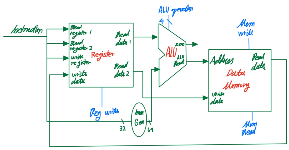
- Ex) sd, rd, offset12 (rs1)
- Read data1 : rs1 값
- Read data2 (write data in data memory) : rd 값
- Immediate 값 : offset 필드의 값을 64-bit Sign-extend
- ALU Result (address) : target memory address
- MemWrite 신호가 1로 바뀌면서 clock edge 발생 → target memory address값에 write data가 store 된다.
-
R type + (load / store) : The data lines cannot be wired together
→ Multiplexers (MUX) are required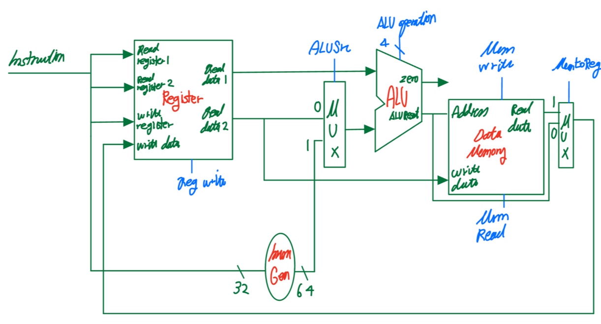
-
Branch instructions
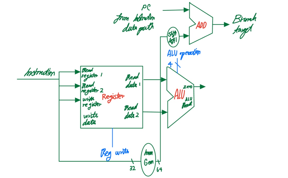
- Ex) beq, rs1, rs2
Loop :
- Read data1 : rs1
- Read data2 : rs2
- ALU operation (subtract) : 같으면 zero flag 1, 다르면 zero flag 0
- zero flag 1이면 branch 해야하는 immediate 값 + 기존 pc 값 from instruction datapath : Branch target
- Ex) beq, rs1, rs2
-
R type + (load / store) + branch
5. Control Signal
- Instruction에 operation의 종류를 구별하는 field (opcode, funct3, funct7) 값들을 조합해서 control signal을 만든다.
-> Control signals derived from instruction. - Complete Single Cycle DataPath
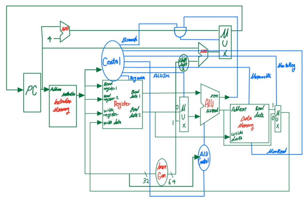
- PCSrc : Branch 여부는 zero flag를 확인해야 가능하다.
-> Branch와 zero flag AND 연산 수행!
- PCSrc : Branch 여부는 zero flag를 확인해야 가능하다.
6. Single Cycle Datapath
- Single Cycle Datapath For R-type Instructions
- Branch : 0
- ALUOp : depends on operation
- MemRead : 0
- MemWrite : 0
- ALUSrc : 0
- MemtoReg : 0
- RegWrite : 1
- Single Cycle Datapath For Load Instructions
- Branch : 0
- ALUOp : ADD
- MemRead : 1
- MemWrite : 0
- ALUSrc : 1
- MemtoReg : 1
- RegWrite : 1
- Single Cycle Datapath For Store Instructions
- Branch : 0
- ALUOp : ADD
- MemRead : 0
- MemWrite : 1
- ALUSrc : 1
- MemtoReg : Don't care
- RegWrite : 0
- Single Cycle Datapath For BEQ(branch) Instructions
- Branch : 1
- ALUOp : Subtract
- MemRead : 0
- MemWrite : 0
- ALUSrc : 0
- MemtoReg : Don't care
- RegWrite : 0
- Single-Cycle implementation 단점 : Longest delay determines clock period.
-> Cannot utilize the resources efficiently - 시험 전 마지막 Data Path